

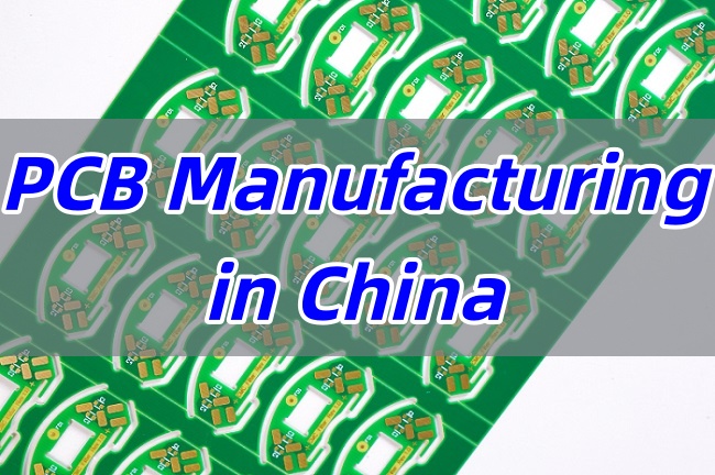
PCB manufacturing in China has become a cornerstone of global electronics, particularly in the 5G and AI era. Companies are challenged by tighter tolerances, higher frequencies, and faster delivery demands. EBest Circuit (Best Technology) addresses these pain points through advanced processes, precision engineering, and comprehensive PCB solutions.
Do any of these challenges of PCB manufacturing in China affect your project?
- Signal Integrity Issues – High-speed 5G and AI boards often face EMI and unstable signals.
- Slow Design-to-Production Cycles – Long prototyping and ramp-up times delay market entry.
- High-Density Board Challenges – Complex HDI boards risk defects and low yield.
- Supply Chain Risks – Component shortages, price volatility, and counterfeit parts disrupt production.
- Reliability Concerns – Thermal stress and soldering defects affect long-term performance.
Here’s the way Best Technology helps the customers overcome them.
- Optimized SI and EMI – Precise impedance control, HDI stacking, and shielding ensure stable signals.
- Rapid Prototyping & Flexible Production – Quick-turn prototypes and scalable manufacturing accelerate time-to-market.
- High-Density Expertise – Laser drilling and AOI improve yield on microvias and multilayer HDI boards.
- Integrated Supply Chain – Centralized procurement and inventory management reduce shortages and risk.
- Strict Quality Assurance – AOI, X-ray, functional testing, and thermal analysis ensure reliability.
At EBest Circuit (Best Technology), we address these challenges with advanced PCB manufacturing capabilities right here in China. Our expertise in high-density HDI boards, high-frequency/low-loss materials, and precise impedance control ensures reliable performance for 5G and AI applications. Combined with rapid prototyping, flexible production, and integrated quality assurance—from AOI and X-ray inspection to functional testing—we help clients bring complex designs to market faster and with technical solutions. For inquiries or to request a quote, contact us at sales@bestpcbs.com.
What is PCB manufacturing in China?
When we ask, “What is PCB manufacturing in China?” the answer extends far beyond simple assembly lines. It represents the core of a global technological ecosystem. To understand its true scale, consider this: the majority of the world’s smartphones, computers, and an increasing share of cutting-edge 5G and AI infrastructure rely on printed circuit boards (PCBs) sourced from China. But this dominance isn’t accidental; it is the result of a mature, sophisticated, and multi-layered industry that has become the undeniable backbone of modern electronics.
So, what exactly is it?
At its heart, PCB manufacturing in China is the large-scale, integrated process of fabricating the essential wiring boards that electronically connect components. However, to define it merely as a production activity is to miss the bigger picture. It is best understood as a comprehensive solution characterized by several key dimensions:
- An Ecosystem of Scale and Integration: It is not just about individual factories but a deeply integrated supply chain. From PCB substrate materials and copper foil to chemical processing and advanced machinery, everything is readily available locally. This creates unparalleled efficiency, drastically reducing time and cost, and making China a one-stop-shop for everything from simple prototypes to complex mass production.
- A Spectrum of Technological Capability: The industry caters to every tier of the market. On one end, online platforms offer incredibly fast and affordable turnkey services for hobbyists and startups. On the other, highly specialized “high-tech companies” produce advanced products like the 4-stage HDI boards essential for 5G microcell antennas and compact wearable devices. This versatility is a key strength.
- A Driver of Innovation: Far from being just a low-cost operator, Chinese PCB manufacturing is a critical enabler of global innovation. The ability to rapidly iterate designs through quick-turn prototyping allows companies in Silicon Valley, Europe, and elsewhere to bring new ideas to life faster. The advanced manufacturing capabilities for high-frequency, high-speed PCBs are directly supporting the global rollout of 5G and AI technologies, which we will delve into in a dedicated section.
- An Evolving High-Tech Industry: The industry has systematically evolved from its roots in labor-intensive production to a capital- and technology-intensive field. Today, it is characterized by extensive automation, rigorous quality control systems compliant with international standards (like ISO, UL, and IATF 16949), and significant investment in R&D. This transformation is what allows it to meet the demanding requirements of modern electronics.
In summary, PCB manufacturing in China is a dynamic and complex force. It is a synergistic combination of unmatched supply chain depth, broad technical prowess, and relentless efficiency that collectively powers global electronics.
What Makes PCB Manufacturing in China Companies Stand Out?
PCB manufacturing in China has rapidly evolved from traditional production facilities to sophisticated, full-service manufacturing hubs. Companies in this industry distinguish themselves not only through technology but also by providing integrated solutions that address complex customer needs. Understanding the key factors that make these companies stand out helps explain why clients worldwide choose Chinese PCB manufacturers like EBest Circuit (Best Technology) for high-performance electronics.
- Advanced Machinery: Investment in automated PCB manufacturing machines, including precision drills, laser direct imaging systems, and automated optical inspection (AOI) tools, reduces defects and ensures consistent quality across production runs.
- Comprehensive Quality Control: Stringent in-process inspection, functional testing, and post-production quality audits minimize failures and improve yield rates. EBest Circuit (Best Technology)’s use of MES systems allows full traceability of components, giving clients confidence in reliability and compliance.
- Flexible Production Capability: Manufacturers can adapt to prototype runs, small batch orders, and large-scale mass production. EBest Circuit (Best Technology) specifically addresses customer pain points by offering scalable solutions without compromising quality or delivery timelines.
- Broad Material and Technology Range: From standard FR4 boards to high-frequency Rogers substrates and advanced HDI/IC substrate boards, Chinese manufacturers cover a full spectrum of materials and technologies, enabling clients to meet diverse performance requirements.
- Integrated Supply Chain: Strong collaboration with local material, component, and equipment suppliers ensures fast procurement, reduced lead times, and cost optimization. This cluster effect supports rapid iteration and innovation, particularly for high-speed and high-frequency electronics.
- Advanced Design and Engineering Support: Many manufacturers, including EBest Circuit (Best Technology), provide engineering assistance for design optimization, impedance control, and thermal management, helping clients avoid common pitfalls and improve product performance.
- Commitment to Certifications and Standards: Leading companies maintain ISO9001, IATF16949, ISO13485, and AS9100D certifications, ensuring compliance with automotive, medical, aerospace, and industrial standards—critical for global customers.
To wrap up, PCB manufacturing companies in China stand out by combining advanced machinery, rigorous quality control, flexible production, broad material and technology expertise, integrated supply chains, and strong engineering support. These advantages allow companies like EBest Circuit (Best Technology) to deliver reliable, high-performance PCB solutions, addressing customer pain points and enabling rapid innovation across global electronics markets.
Top PCB Manufacturers in China
China has become a global leader in PCB manufacturing, with a wide range of companies offering diverse capabilities from simple double-sided boards to advanced HDI and substrate-integrated designs. These top manufacturers distinguish themselves through technology, quality control, innovation, and comprehensive service, helping clients worldwide meet the demands of high-performance electronics.
1. EBest Circuit (Best Technology)
- EBest Circuit (Best Technology) is recognized as one of China’s leading PCB manufacturers.
- The company offers a full spectrum of services, including PCB design, prototyping, multilayer fabrication, and assembly.
- With advanced machinery, MES traceability systems, and engineering support, EBest Circuit (Best Technology) addresses customer pain points such as tight schedules, complex designs, and high-quality requirements.
2. Shenzhen Fastprint Circuit Co., Ltd.
- Shenzhen Fastprint is known for high-precision PCB production and fast-turn prototyping services.
- The company specializes in HDI boards, flexible PCBs, and high-frequency circuits, catering to telecom, automotive, and industrial sectors.
- Fastprint emphasizes short lead times and quality certifications, making it a reliable partner for global electronics clients.
3. Kingboard PCB Technology Co., Ltd.
- Kingboard is one of the largest PCB producers in China, with extensive experience in multilayer and high-density boards.
- The company provides both standard FR4 PCBs and advanced high-speed/low-loss materials for telecom and industrial applications.
- Kingboard’s global presence and large-scale manufacturing capacity make it ideal for clients requiring high-volume production.
China’s top PCB manufacturers combine advanced technology, rigorous quality control, flexible production, and comprehensive engineering support. These companies not only produce high-quality PCBs but also provide integrated solutions that help clients address complex design challenges, accelerate time-to-market, and support innovation in sectors such as 5G, AI, and high-speed computing
Understanding the PCB Manufacturing Process in China
Double-sided PCBs are among the most common types of circuit boards used in electronic products. Although the production process is relatively standardized, each step requires strict control to ensure precision, reliability, and stable functionality. Below is a detailed explanation of the typical double-sided PCB manufacturing process in China.
1. Material Cutting (Substrate Preparation)
- Cut the base material according to design files and production requirements.
- Ensure the material meets FR4 or other substrate specifications, providing a stable foundation for subsequent processes.
2. Drilling
- Mechanical or CNC drilling is used to create through-holes for electrical connectivity.
- High precision is required, especially for proper alignment of holes on double-sided boards.
3. Copper Deposition & Board Plating
- Copper is deposited on the hole walls to form electrical connections.
- Board surface is electroplated with copper to increase thickness, providing stable conductors for circuit patterns.
4. Circuit Patterning (Exposure → Development → Etching)
- Apply photoresist and use photolithography to define the circuit layout.
- Develop to remove unexposed photoresist.
- Chemical etching removes excess copper, leaving only the desired circuitry.
5. AOI (Automated Optical Inspection)
- Inspect circuit integrity and detect defects such as breaks, shorts, or pattern errors.
6. Solder Mask (Exposure → Development)
- Apply solder mask to protect the circuit and prevent solder bridging.
- Use exposure and development to accurately define protected areas.
7. Silkscreen Printing
- Print component identifiers, logos, and other markings for assembly and traceability.
8. Baking / Curing
- Bake the board to cure the photoresist and solder mask layers, enhancing stability.
9. Surface Finish
- Apply surface finishes such as ENIG, HASL, or OSP based on client requirements to improve solderability and durability.
10. Routing & Profiling
- Cut or V-score the boards to final dimensions, achieving precise shape and size.
11. Electrical Testing
- Conduct electrical tests to verify circuit continuity and impedance stability.
12. FQC (Final Quality Control)
- Perform comprehensive checks on appearance, dimensions, markings, and functionality.
- Ensure compliance with customer and international standards.
13. Packaging & Warehousing
- Protect finished boards with anti-static and moisture-proof packaging.
- Store properly for shipping or further assembly.
In essence, the double-sided PCB manufacturing process involves a series of tightly controlled steps, from substrate preparation and drilling to surface finishing and final inspection. Each stage directly affects the quality and reliability of the board. By strictly executing these processes, combined with automated inspection and professional management, Chinese PCB manufacturers can deliver consistent, high-quality products that meet the demanding requirements of the global electronics industry.
Are Printed Circuit Board Manufacturers in China of 4-Stage HDI Boards Regarded as High-Tech Companies?
The answer is unequivocally yes. Manufacturers capable of reliably producing advanced 4-layer HDI boards are not mere suppliers—they are at the forefront of electronic innovation and serve as strategic technical partners. Mastery of this complex process is a hallmark of high-tech companies, distinguishing them from standard PCB manufacturers. At EBest Circuit (Best Technology), this positioning is supported by three core pillars: continuous R&D investment and advanced equipment, deep proprietary process knowledge, and a key role in driving next-generation technology development.
1. Technological Benchmark: Advanced Manufacturing Capabilities
- Sequential Lamination and Laser Drilling: Unlike standard multilayer PCBs, 4-layer HDI boards require multiple lamination cycles. Each layer is precisely drilled using ultrafast CO2 or UV lasers at micron-level accuracy. This enables staggered microvia structures, which are critical for high-density components such as modern BGAs.
- Any-Layer Interconnection (ALI): ALI represents the pinnacle of HDI technology. Each insulating layer can be interconnected through laser microvias, maximizing routing density in minimal space. This demands unparalleled alignment precision throughout the manufacturing process.
- Advanced Materials Expertise: High-performance 4-layer HDI boards for 5G or AI applications often use specialized low-loss or high-frequency laminates. EBest Circuit (Best Technology) possesses proprietary techniques to handle these demanding materials effectively.
2. Knowledge Assets: Proprietary Process Expertise
- Proprietary Process Recipes: Beyond equipment, EBest Circuit (Best Technology) embeds intellectual property into its manufacturing. Optimized laser energy settings, etching chemistries, and plating parameters ensure flawless via formation and defect-free layer connections, even with challenging materials.
- Data-Driven Process Control: Statistical process control monitors every critical step. This data-centric approach enables predictive maintenance and continuous improvement, going far beyond simple pass/fail inspection.
- Design for Manufacturability (DFM) as a Service: EBest Circuit (Best Technology) provides value-added DFM feedback, advising on optimal lamination structures, via types, and routing strategies. This consultancy approach reinforces the company’s role as a technical partner, not just a manufacturer.
3. Strategic Impact: Enabling Next-Generation Applications
- 5G Infrastructure: Miniaturization and signal integrity requirements for 5G millimeter-wave antennas and network devices depend on our 4-layer HDI high-density interconnect solutions.
- Artificial Intelligence and High-Performance Computing: AI accelerators and HPC servers require massive processing power in compact packages. EBest Circuit (Best Technology)’s 4-layer HDI boards route thousands of high-speed differential pairs from processors and memory while managing substantial thermal loads.
- Advanced Medical and Aerospace Electronics: High-reliability, compact designs for medical imaging equipment and aerospace electronics are achievable only with our advanced HDI solutions.
To draw this to a close, Chinese PCB manufacturers specializing in 4-layer HDI boards, such as EBest Circuit (Best Technology), clearly qualify as high-tech enterprises. Their advanced manufacturing capabilities, combined with proprietary knowledge and innovation-driven services, enable the consistent production of high-density, high-performance, and highly reliable HDI boards. This makes them indispensable partners for clients in 5G, AI, HPC, medical, and aerospace sectors.
By leveraging ongoing R&D investment, proprietary process expertise, and deep understanding of next-generation technology demands, EBest Circuit (Best Technology) provides end-to-end solutions—from design optimization to high-end manufacturing—that ensure performance, reliability, and rapid time-to-market. Far from being just a supplier, we serve as a strategic technical partner driving innovation and enabling clients to confidently tackle the most complex electronic challenges.
How Is PCB Manufacturing in China Adapting to the Era of 5G and AI?
The advent of 5G and Artificial Intelligence (AI) demands a fundamental shift in printed circuit board (PCB) design and manufacturing. These technologies require boards that can handle higher frequencies, greater data densities, and increased thermal loads. Chinese PCB manufacturers are not merely keeping pace with these demands; they are actively driving innovation through strategic investments in three core areas: advanced materials, precision engineering, and agile production methodologies. This section details how these adaptations provide a critical competitive edge for clients developing next-generation products.
Mastery of Advanced High-Frequency and High-Speed Materials
The transition to 5G millimeter-wave (mmWave) frequencies makes signal integrity the paramount concern. Chinese leading manufacturers have deeply invested in expertise and processing capabilities for specialized materials that are essential for high-frequency performance.
- Beyond FR-4: While standard FR-4 remains adequate for many applications, high-speed digital (AI processors) and RF (5G antennas) circuits require low-loss materials. Top manufacturers are proficient with a range of advanced substrates:
- Low-Loss Thermoplastics: (e.g., Rogers RO4000® series, Taconic TLY) for optimal high-frequency signal transmission with minimal loss (low Df – dissipation factor).
- Hydrocarbon Ceramics: (e.g., Rogers RO3000® series) offering excellent temperature stability and a stable dielectric constant (Dk), which is critical for consistent impedance.
- Polyimide and LCP: For flexible PCBs in high-frequency applications like mmWave antennas, where flexibility and performance are both required.
- Material Partnership and Selection Guidance: Trusted manufacturers don’t just stock these materials; they provide valuable Design for Manufacturability (DFM) feedback. They advise clients on the most cost-effective and performance-appropriate material choice for a specific application, preventing over-engineering or performance bottlenecks.
Precision Engineering for Signal and Power Integrity (SI/PI) and Thermal Management
Success in the 5G/AI era hinges on controlling the physical behavior of the PCB. Chinese top-tier manufacturers have implemented rigorous engineering processes to ensure this control.
- Precision Impedance Control: As you correctly noted, impedance control is non-negotiable. Leading factories utilize sophisticated field solvers for simulation and maintain tight process controls to achieve tolerances of ±10% or better. They work with clients to define stack-ups and trace geometries that meet the target impedance, as defined by formulas like the microstrip line equation: Z₀ = (87 / √(εr + 1.41)) * ln(5.98h / (0.8w + t)), which provides a more practical calculation accounting for trace thickness (t).
- Advanced Thermal Management Solutions: AI processors and 5G power amplifiers generate significant heat. Manufacturers address this through:
- Thermal Vias and Heatsinks: Designing and implementing complex via structures (staggered, stacked) under BGA packages to efficiently conduct heat away from critical components.
- Thermal Simulation Support: Offering pre-production thermal simulation services to identify potential hotspots and validate the board’s thermal design, preventing field failure.
- Specialized Constructions: Manufacturing boards with heavy copper layers (≥3 oz) for higher current carrying capacity and using metal core (IMS) or insulated metal substrates (IMPCB) for superior heat dissipation in high-power LED and RF applications.
Agile Prototyping, Integrated Testing, and Data-Driven Quality
The rapid iteration cycles of AI and 5G development require a manufacturing partner that can move with equal speed and confidence.
- Rapid, High-Fidelity Prototyping: The ability to quickly produce prototypes using production-intent materials and processes is crucial. Chinese manufacturers excel at providing ”first-time-right” prototypes that accurately represent the final product’s performance, allowing for meaningful validation and testing.
- Comprehensive and Integrated Testing Regimens: To ensure reliability, advanced manufacturers deploy a multi-layered testing strategy:
- Advanced Electrical Testing: High-frequency network analyzer testing to validate S-parameters (e.g., Insertion Loss, Return Loss) for RF boards.
- Automated Optical Inspection (AOI) and AXI: 3D AOI and Automated X-ray Inspection to detect hidden defects in complex HDI and BGA assemblies.
- Time-Domain Reflectometry (TDR): Used to accurately measure and verify controlled impedance on the actual manufactured board, providing data-backed confirmation of signal integrity.
- Data-Driven Process Control: Trust is built on verifiable quality. Leading manufacturers employ Statistical Process Control (SPC) and provide comprehensive certification data packs with each order, which may include impedance test reports, quality certifications, and even x-ray images, offering full traceability and proof of compliance.
To summarize, by mastering these three pillars—advanced materials, precision engineering, and agile, data-verified production—Chinese PCB manufacturers have positioned themselves as indispensable partners in the 5G and AI revolution. They offer clients the technical capability to push performance boundaries while mitigating risk and accelerating time-to-market.
How PCB Assembly in China Enhances Electronics Manufacturing?
The term “electronics manufacturing” often evokes images of large-scale consumer electronics production. However, the true value of PCBA in China extends far beyond mass production. Its core strength lies in the seamless integration of scale, technical expertise, and supply chain coordination, transforming designs into reliable, market-ready products efficiently and cost-effectively. For global enterprises, this translates into a decisive competitive advantage.
1. Unmatched Scalability and Flexibility: From Prototyping to Mass Production
Chinese PCBA providers excel in agile manufacturing, supporting products throughout their entire lifecycle.
- Rapid Prototyping and New Product Introduction: Leading manufacturers operate dedicated lines for fast prototyping, enabling global R&D teams to complete design iterations within days and significantly shorten time-to-market. Engineering support during NPI includes design-for-manufacturability (DFM) analysis, optimizing component placement to eliminate potential production issues.
- Smooth Capacity Ramp-Up: Clients can transition seamlessly from 10 prototype units to tens of thousands in mass production with a single partner. Advanced production planning and buffer stock strategies ensure supply chain resilience and minimize disruptions.
2. Precision Processes Ensuring Superior Quality
Beyond basic surface-mount technology (SMT), advanced assembly facilities deploy a range of processes to guarantee the reliability of complex products.
- Advanced Soldering Techniques: For mixed-technology boards, selective wave soldering ensures robust connections for connectors while protecting delicate SMD components. For more precise assemblies, hot-air reflow with precise thermal profiling prevents heat-related stress damage.
- Comprehensive Inspection Systems: Multi-tiered quality control ensures defect-free assemblies:
- Automated Optical Inspection (AOI): Scans every solder joint for defects.
- X-Ray Inspection (XRI): Checks hidden solder joints under BGA and other encapsulated components.
- In-Circuit and Functional Testing: Verifies electrical characteristics and performance under simulated operational conditions.
3. Strategic Value of One-Stop Solutions
The greatest advantage of Chinese PCBA lies in simplifying supply chain complexity. Integrated “PCBA++” or full product assembly models deliver significant value:
- Component Sourcing and Management: Leveraging purchasing scale and local market access, manufacturers secure components competitively while effectively managing inventory to mitigate shortages or counterfeit risks.
- End-to-End Accountability: Managing PCB fabrication, component sourcing, assembly, final product integration, and logistics within a single ecosystem centralizes responsibility, reduces management overhead, and prevents finger-pointing across multiple suppliers.
- Optimized Lead Times: Consolidating manufacturing, assembly, and testing within one ecosystem drastically reduces logistics delays. Processes that would normally take weeks across a fragmented supply chain are condensed into a single streamlined workflow.
As a final remark, PCBA in China elevates electronics manufacturing by acting as an enabler of innovation and efficiency. It offers companies rapid innovation agility, the technical ability to produce complex products, and supply chain advantages that accelerate market entry while controlling costs. This integration makes Chinese PCBA an indispensable strategic partner for global electronics enterprises seeking speed, reliability, and competitiveness.
What Certifications Should Printed Circuit Board Manufacturers in China Have?
For global clients, choosing a PCB manufacturer in China is not just about cost or production speed. Certifications act as proof that a company follows international quality standards and can deliver reliable products. They reduce regulatory risks, ensure consistent quality, and provide confidence in critical applications such as automotive, medical, aerospace, and industrial electronics. EBest Circuit (Best Technology) exemplifies this approach by maintaining multiple internationally recognized certifications.
1. ISO 9001 – Quality Management System
- ISO 9001 certifies that a company has a structured quality management system in place.
- It ensures processes are documented, monitored, and continuously improved.
- Customer Value: Clients benefit from consistent board quality, reduced defects, and predictable production performance.
2. IATF 16949 – Automotive Standard
- This standard is specific to automotive electronics manufacturing, emphasizing defect prevention and continuous improvement.
- It integrates process risk management, traceability, and supplier control.
- Customer Value: Automotive clients can trust that their PCB supplier meets rigorous industry safety and reliability requirements.
3. ISO 13485 – Medical Device Quality
- ISO 13485 focuses on design, production, and servicing of medical devices.
- It requires strict traceability, controlled processes, and risk management.
- Customer Value: Medical electronics clients gain confidence that PCBs meet hygiene, reliability, and compliance standards critical for patient safety.
4. AS9100D – Aerospace Standard
- AS9100D extends ISO 9001 requirements to aerospace manufacturing.
- It covers product safety, documentation, supplier management, and quality control at every step.
- Customer Value: Aerospace clients can rely on high-precision, high-reliability boards for critical systems.
5. Implementation and Benefits in EBest Circuit (Best Technology)
- EBest Circuit (Best Technology) integrates these standards into daily operations using MES systems, automated inspection, and documented quality checks.
- Customers experience end-to-end traceability, reduced regulatory risk, and boards that consistently meet specifications.
- These certifications also ensure that new products, such as high-frequency 5G or HDI boards, are produced with controlled processes and predictable outcomes.
To conclude, selecting a PCB manufacturer with internationally recognized certifications is crucial for reducing risk and ensuring high-quality output. EBest Circuit (Best Technology)’s adherence to ISO 9001, IATF 16949, ISO 13485, and AS9100D demonstrates its commitment to quality, reliability, and compliance. For clients in automotive, medical, aerospace, and industrial sectors, these certifications provide assurance that every PCB delivered meets stringent standards and performs reliably in critical applications.
High-Quality PCB Made in China by EBest Circuit (Best Technology)
Producing reliable, high-performance PCBs in China requires more than standard fabrication—it demands precision, flexibility, and deep technical expertise. EBest Circuit (Best Technology) has established itself as a trusted partner for clients facing high complexity, tight tolerances, and critical applications. Through advanced capabilities and customer-focused service, every PCB meets international quality standards and specific client requirements.
1. Precision Manufacturing Beyond Standards
- Expertise in Advanced PCB Types: EBest Circuit (Best Technology) excels in HDI, high-frequency/high-speed boards, thick copper, and rigid-flex combinations.
- Solving Complex Design Challenges: Advanced processes, including laser drilling, controlled impedance, and multilayer lamination, allow clients to overcome design complexity and EMI issues.
- Quality Assurance: Strict process control and in-line inspections reduce defects and improve yields, even for highly demanding projects.
2. Seamless End-to-End Service Experience
- One-Stop Solutions: From design support and rapid prototyping to large-scale production and international logistics, clients enjoy a complete service chain.
- Time and Cost Efficiency: Integrated operations shorten lead times and reduce management overhead, allowing clients to focus on product development and market delivery.
- Production Flexibility: Capable of handling prototype, small batch, and mass production without compromising quality or delivery schedules.
3. Customer-Centric Collaboration Model
- Dedicated Project Management: Each client is assigned a project manager to oversee production, ensuring transparency and timely updates.
- Proactive Design Optimization: Engineers provide value-added recommendations for layout, material selection, and signal integrity to enhance board performance.
- Building Partnerships: Emphasizes collaboration rather than mere service, fostering trust and long-term relationships.
4. Driving 5G and AI Projects
- Specialized 5G/AI PCB Expertise: EBest Circuit (Best Technology) designs and manufactures high-frequency, high-speed boards suitable for 5G base stations, antenna modules, and AI accelerators.
- Ensuring Signal Integrity and Reliability: Strict impedance control, multilayer HDI stacking, and EMI optimization guarantee performance in complex applications.
- Customer Benefit: Clients can confidently entrust critical 5G and AI projects to EBest Circuit (Best Technology), enjoying full support from design to large-scale delivery.
5. Integrated PCBA Manufacturing Capability
- In-House PCBA Factory: EBest Circuit (Best Technology) operates its own PCBA production facility, enabling full control over assembly quality and process integration.
- Advanced Assembly Techniques: Surface-mount (SMT), through-hole, mixed-technology boards, and high-density assemblies are handled with precision to meet complex customer requirements.
- End-to-End Oversight: From PCB fabrication to complete assembly, including functional testing and quality verification, clients benefit from a single-source solution that guarantees consistency and reliability.
To put it simply, through precision manufacturing, end-to-end service, customer-focused collaboration, and specialized 5G/AI PCB capabilities, EBest Circuit (Best Technology) delivers high-quality PCBs made in China. Clients gain not only reliable and precise boards but also faster time-to-market, optimized performance, and strong technical support, making EBest Circuit (Best Technology) the preferred partner for companies tackling high-complexity and mission-critical electronic applications.
Case of PCB Manufacturing at EBest Circuit (Best Technology)
Case 1: 4-Layer Rigid-Flex PCB for 5G Wearable Devices
Board Specifications:
- Board Type: 4-layer Rigid-Flex PCB
- Flexible Layer Material: 18/25μm double-sided ED, adhesive-free
- Rigid Layer Thickness: 0.55 mm ±10%
- Flexible Layer Thickness: 0.11 mm ±0.03 mm
- Surface Finish: ENIG 1μ”
- Standard: IPC Class 2
This advanced rigid-flex PCB exemplifies how EBest Circuit (Best Technology) enables 5G innovation in wearable technology. The board’s unique combination of rigid and flexible sections allows for:
- Space Optimization: Enables compact, lightweight designs for 5G smartwatches and AR/VR headsets
- Signal Integrity: The adhesive-free flexible layer maintains stable impedance critical for 5G mmWave frequencies
- Reliability: Withstands constant bending in wearable devices while maintaining 5G connectivity
Case 2: 4-Layer FR4 PCB for 5G Small Cell Base Stations
Board Specifications:
- Board Type: 4-layer FR4 PCB
- Material: TG170, S-10002M
- Copper Thickness: 1 oz / 0.5 oz / 0.5 oz / 1 oz
- Board Thickness: 1.6 mm ±10%
- Surface Finish: ENIG (Au 1μ”)
This high-temperature FR4 PCB demonstrates EBest Circuit (Best Technology)’s contribution to 5G infrastructure:
- Thermal Management: TG170 material ensures stability in high-power 5G small cell applications
- Impedance Control: Precision layer stacking enables reliable high-frequency signal transmission
- Durability: Black solder mask provides superior UV resistance for outdoor 5G deployments
EBest Circuit (Best Technology)’s manufacturing capabilities directly address key 5G requirements:
- High-Frequency Performance: Precision impedance control supports 5G’s millimeter-wave bands
- Miniaturization: Advanced rigid-flex technology enables compact 5G device designs
- Reliability: IPC Class 2 standards ensure consistent performance in demanding 5G applications
- Thermal Management: High-Tg materials maintain stability in power-intensive 5G equipment
These case studies demonstrate how EBest Circuit (Best Technology)’s precision manufacturing capabilities are essential for overcoming the technical challenges of 5G implementation, from consumer wearables to infrastructure equipment.
To wrap things up, PCB manufacturing in China is evolving in response to the demands of 5G and AI. EBest Circuit (Best Technology) offers advanced processes, expert engineering, and turnkey solutions to address customer pain points, including delayed deliveries, low yields, and signal integrity challenges. If you would like to get a quote for your PCBs, pls contact us at sales@bestpcbs.com.
Tags: Manufacturing in China