3) Laminate trace layer and copper core layer together.
a. Add glue on bottom side of trace layer so that it be stick on copper core
b. CNC milling/routing the trace layer with glue, to remove the cutout where the convexity of copper core will be.
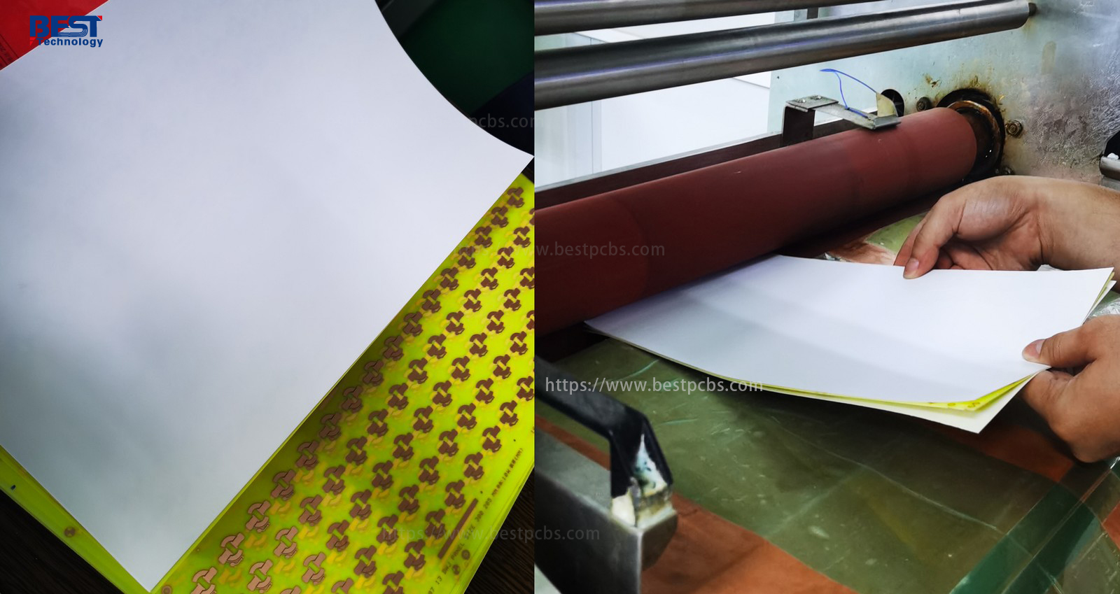
c. Take off the white release paper, align and put the trace layer on copper core
 Trace layer before aligning on copper core
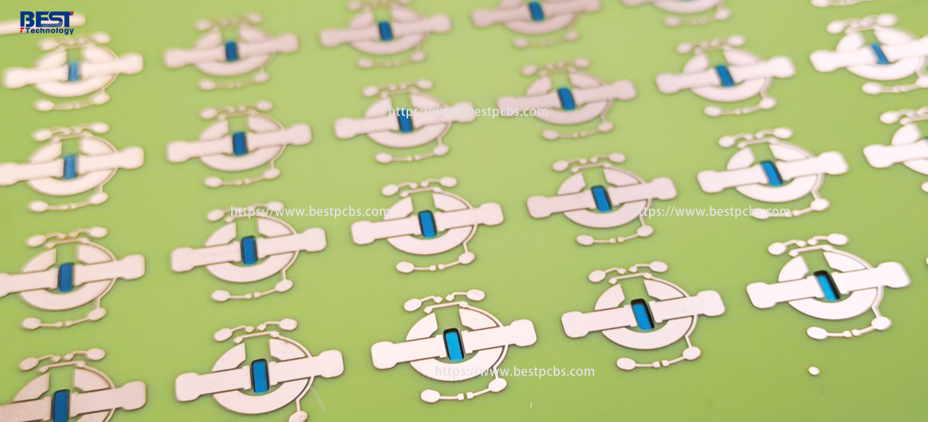
(trace layer & convexity aligning process 2)
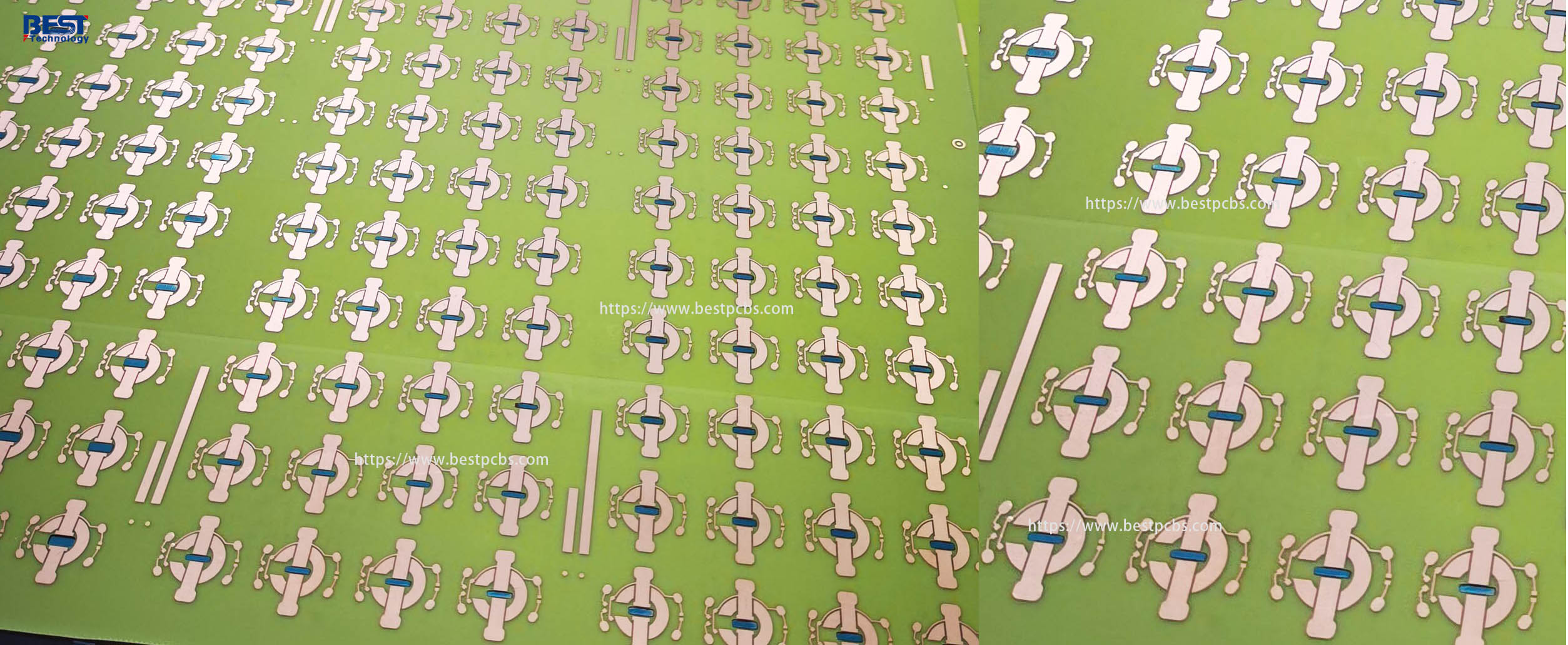 (trace layer & convexity aligning process 2)
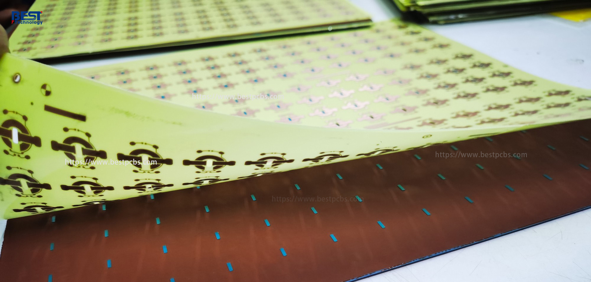
c. Lamination process: separate each layer with high temperature paper and silicon gel, and put them into high temperature laminator with vacuum condition. After several hours with suitable parameters, the trace layer and copper core will be stick to each other firmly and become a new board, like normal single layer or double sided MCPCB.
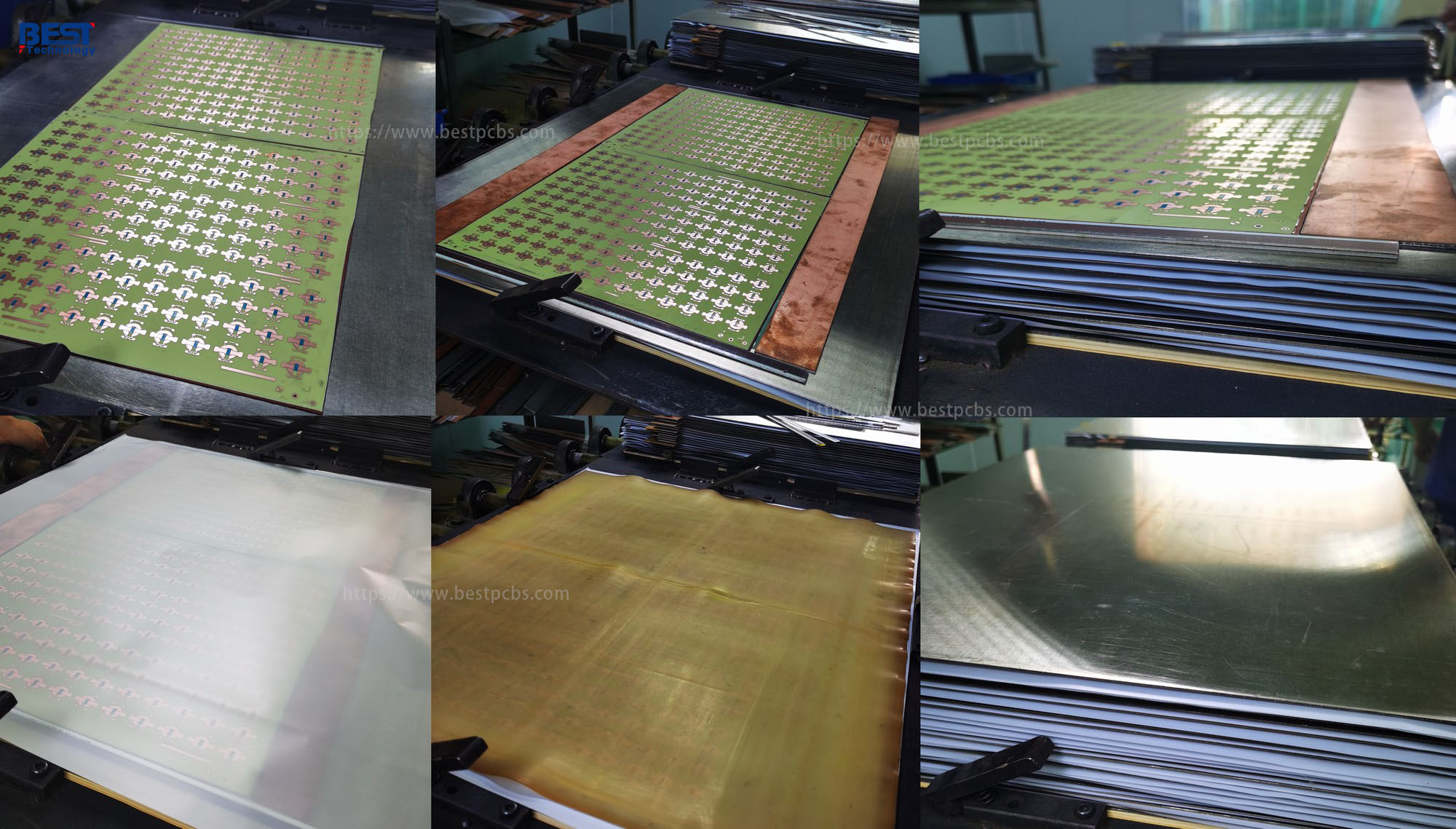 (lamination process: laminate & align board before hot process lamination)
d. SinkPAD come out.
After these steps, you can see, the electronics connection will be on trace layer and then the direct thermal conducting PAD is coming from copper core. And the trace PAD on trace layer seemed in the sink area of copper core, so it named “SinkPAD board” or “SinkPAD PCB”.
Also because the electronic related function was on trace layer and thermal conduction was on copper core, they are separated from each other. So that layer also named as Thermoelectric separation circuit board.
By this way, the thermal PAD of LED can be touched the copper PAD and core directly, so that heat can be conducting directly from LED to copper core, so it is also named as DTP (Direct Thermal Path). By this way, we can reach 400W/m.K thermal conductivity.