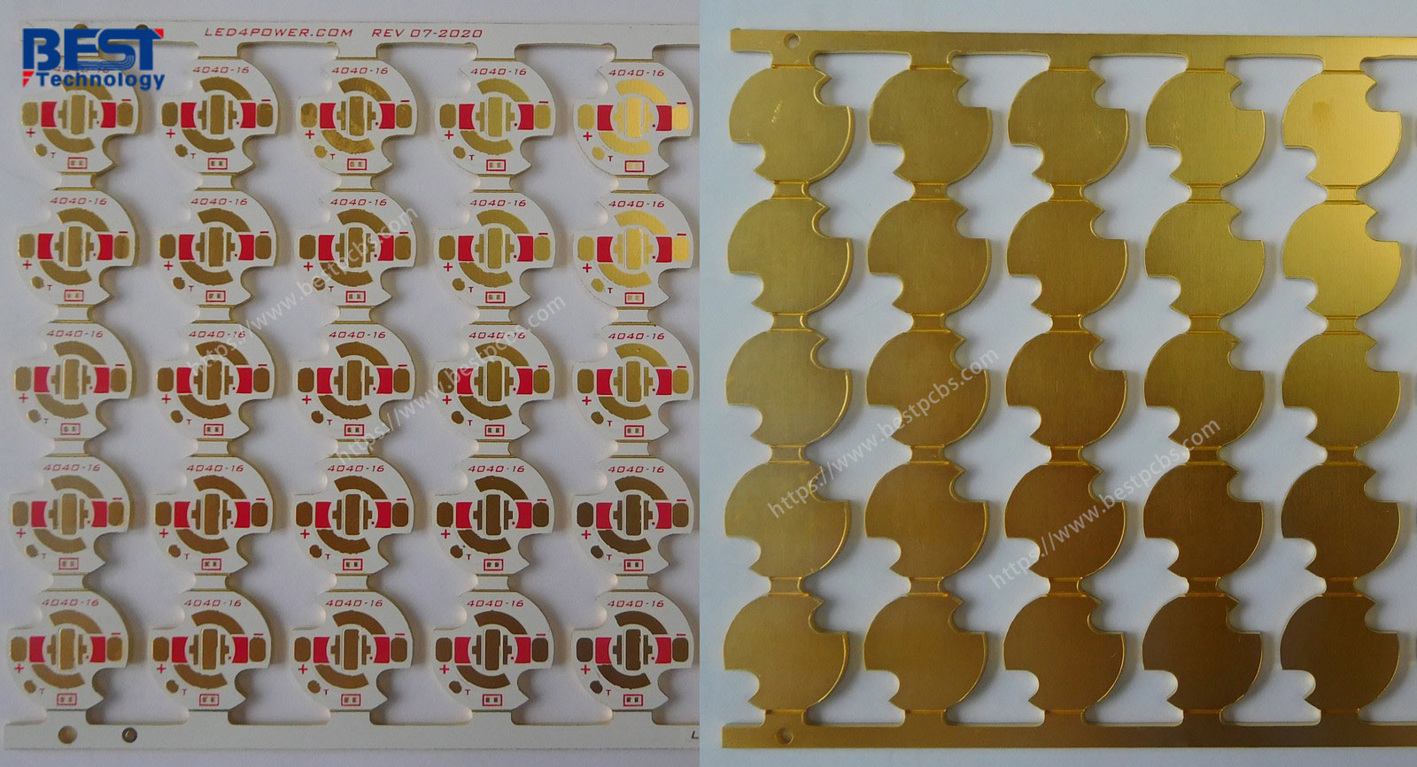
 (top and bottom view of finished SinkPAD board- in panel)
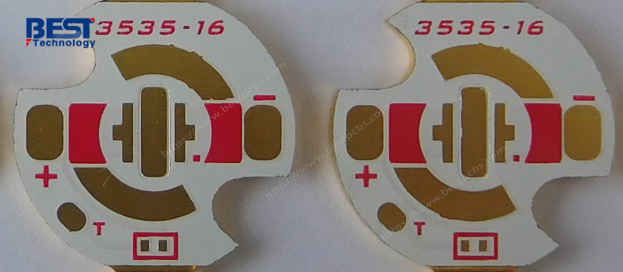 (top and bottom view of finished SinkPAD board- in single piece)
To be noted that the thickness of trace layer with glue is 0.20mm and the depths of copper/thickness of convexity is also 0.20mm, but considering manufacturing process, there’ll be a +/-0.05mm thickness tolerance comparing trace layer and convexity. And this is one of reason why you see the uneven of finished board.
Also the distance between edge of trace layer cutout and edge of convexity of copper is +/-0.10mm, so you can see the gap between in finished board, even it’ll be covered by soldermask.
If you still have any question on the manufacturing process of our SinkPAD board, welcome to contact us any time!