|
The detail steps after printing as below. If you still have questions about the Sample making, please click here to read more: Sample making (1)Spreading: After printing, put aside the product for 5 to 7 minutes until the netted texture is gone. Ceramic PCB is going through the firing oven.(The tray is made of material with high temperature resistant because of the high temperature in the firing oven.) 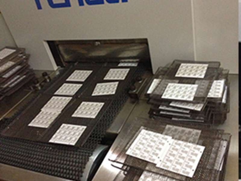
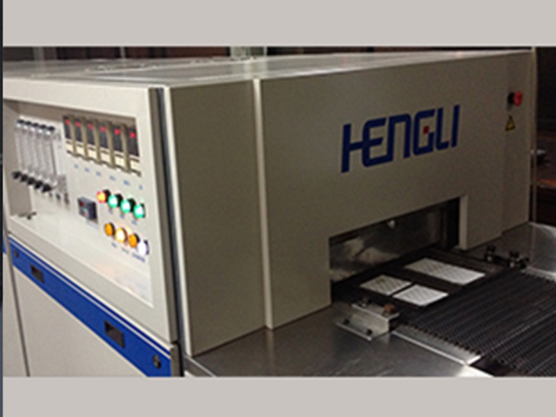
It is required to pass through the baking oven to dry the surface of the conductive ink in three cases: 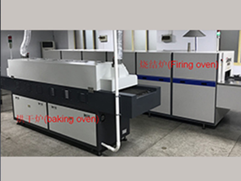
Then we are going to the next step Printing resistance ink and laser resistor trimming |