





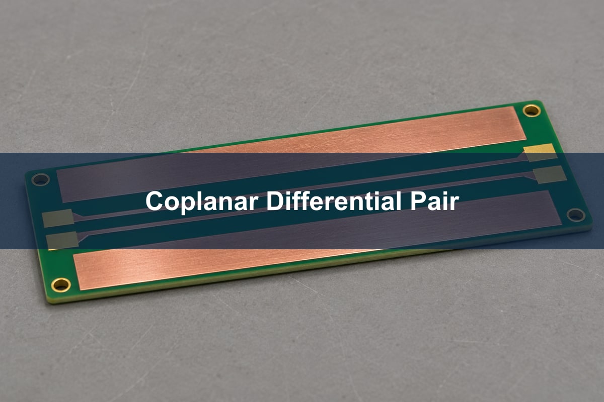
A coplanar differential pair has two signal traces and nearby reference copper on the same PCB layer. If you move that copper close to an existing pair, do not reuse the old impedance result. The gap to ground becomes part of the cross-section, along with the gap between traces and the distance to any reference plane underneath.
Suppose an engineer has sized a surface differential pair above a continuous plane, then adds ground copper beside it to fit a connector escape. The decision is not simply whether ground copper is good or bad. It is whether the final layout still matches the model used to set the trace width and gaps. Here is how to check that from the stackup through the test report.
Coplanar differential pair meaning: Which copper counts?
“Differential” describes how the two signals work together; “coplanar” describes where the reference copper is placed. In differential operation the two conductors carry opposite signals. A nearby conductor still affects the electric field, even though the two signal traces are coupled to each other. Two traces on the same layer are not, by themselves, what a PCB calculator means by a coplanar pair.
Open the final copper view and look across a straight section of the pair, not just at its net names. Identify the gap between the signals and the gap from each signal to its outside ground copper. Then open the stackup and identify any reference plane above or below. These are separate inputs. A calculator icon is useful only if it shows the same arrangement.
Coplanar differential pair vs non coplanar: Which model fits?
Choose the model that matches the board. A conventional surface pair over a plane can be modeled as edge-coupled microstrip when nearby side copper is absent or shown to have negligible effect. A grounded coplanar pair has both adjacent ground and a reference plane. It gives the designer another geometry variable, but that variable also has to be controlled in fabrication.
| Cross-section | Reference geometry | When to use the model |
| Edge-coupled microstrip | Plane below; no significant side copper | The approved layout keeps neighboring copper far enough away for the modeled tolerance |
| Grounded coplanar pair | Side grounds and a plane below | Both sets of references are present in the routed cross-section |
| Coplanar pair without backing plane | Side grounds; no continuous lower plane in the modeled region | The stackup really lacks that plane and the tool supports this structure |
In the example, keep width, pair spacing, material and bottom plane unchanged. In version A, side copper is pulled back and a sensitivity check shows its effect is immaterial: retain the microstrip model. In version B, move only the side copper inward: rerun the model with both side grounds present. If the result leaves the project’s impedance window, change the geometry or restore the keepout. Do not adopt a universal clearance multiple in place of that check.
Key dimensions of a differential coplanar waveguide with ground
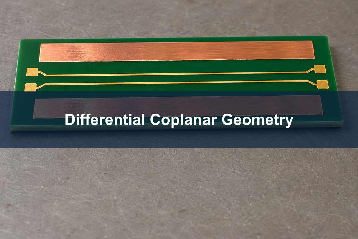
The parameter that is easiest to miss is the side-ground clearance. Measure it from the outside edge of each signal trace to the adjacent copper edge, separately from the edge-to-edge spacing inside the pair. The table gives the inputs to collect before asking a solver for an answer; it deliberately does not prescribe a universal width or gap.
| Input | Where to obtain it | Why it changes the answer |
| Finished trace width and copper thickness, mm | Fabricator’s impedance proposal or approved stackup | Finished geometry differs from a nominal copper weight or artwork width |
| Pair spacing and both side-ground clearances, mm | Final copper or fabrication artwork; confirm edge-to-edge convention | Pair coupling and side-ground coupling are separate effects |
| Dielectric height and Dk | Approved stackup and material model | Use the height to the actual reference and the appropriate dielectric value, not overall board thickness |
| Solder mask and local geometry | Final mask artwork and solver model | Coating and asymmetric copper can change what the simple cross-section represents |
For the same pair, a plane on the next layer is not equivalent to a plane across the entire board thickness. Locate the actual signal and reference layer identifiers on the approved stackup. If the far-side plane is broken at the connector, mark that transition for separate review; a uniform 2D model does not evaluate the break.
What to enter in a coplanar differential pair impedance calculator
Compare two calculators only after making their cross-sections and inputs equivalent. Start with the reference layers, finished dielectric height and copper thickness, then check Dk, mask, trace width, pair gap and outer gap. One tool may include mask or side copper in a way the other does not. Altium’s impedance documentation describes both the coplanar models and input differences that can explain disagreement.
Save an input sheet with units and a cross-section sketch, then change one parameter at a time in the same tool. This is more useful than averaging two outputs. If a calculator assumes symmetry but the real layout has ground much closer on one side, use a model that supports the actual geometry. At pads and layer changes, supplement the cross-section model with a suitable transition analysis or measurement.
Differential pair impedance formula
For a symmetric pair in odd-mode excitation, differential impedance is twice the odd-mode impedance of one line: Zdiff = 2 × Zodd. It is not necessarily twice the impedance of an isolated trace, because the neighboring signal and reference copper affect the fields.
For a teaching example, take a project target of 100 Ω ±10%, not a universal interface requirement. Its acceptance window is 90–110 Ω. If a symmetric model returns 48 Ω odd mode, the calculated differential impedance is 96 Ω. If a second model of the same pair with closer side copper returns 44 Ω odd mode, the result is 88 Ω. Those input values illustrate the decision and are not solver predictions for a specific geometry. The first result is in the window, the second is not; neither replaces a tolerance analysis or measurement.
Differential pair routing guidelines
Keep the final pair and its references consistent with the modeled profile. Repour copper and inspect the finished artwork before release: a ground island, neckdown, asymmetric clearance or plane split can appear after the initial routing check. Length matching does not make those cross-section changes disappear.
For the connector escape in the example, mark where the narrow fanout begins and ends. If the required ground clearance cannot be maintained there, review it as a local transition rather than applying a new trace width to the entire route. Check that adjacent copper is tied to the intended reference and that layer changes have an appropriate return path. Use the microstrip PCB guide for the underlying plane-referenced geometry.
What a PCB impedance test coupon can verify
A coupon is useful only when it represents the structure you intend to accept. For the coplanar route, ask the fabricator to identify the coupon’s stackup revision, signal layer, reference layers, pair spacing and side-ground arrangement. A coupon for ordinary differential microstrip can pass while saying nothing about a nearby-ground variant.
Check the impedance report against the fabrication drawing: match the coupon ID to the layer and geometry, confirm the target and tolerance, and identify the evaluated segment. If the report only shows “100 Ω pass” with no link to the modeled construction, request the coupon mapping and trace before accepting it as evidence for the coplanar pair.
How to read a differential TDR measurement
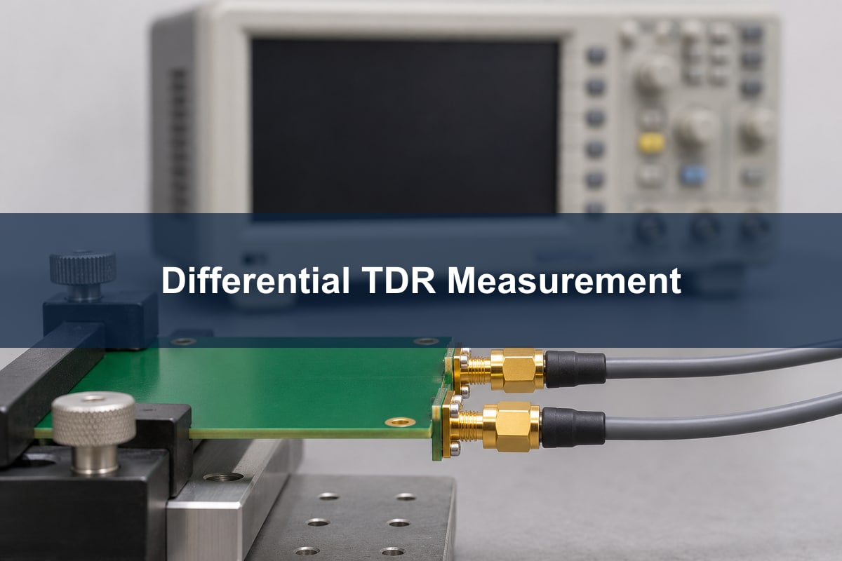
A differential time-domain reflectometry (TDR) trace shows impedance changes along a path under differential stimulus. Agree on the fixture or launch reference, the part of the trace to evaluate and the pass window before comparing results. A connector discontinuity near the launch should not be mistaken for the steady region of a uniform coupon.
If the coupon is in range but the assembled link still fails, do not immediately change the straight-line width. Compare the actual launch, return path, layer changes and connector geometry with what the coupon omits. Use an appropriate link-level test for the required signal behavior. A passing coupon supports impedance control of the represented cross-section; it does not certify loss, mode conversion or the performance of the assembled channel.
FAQ
Can I leave a floating copper pour beside the pair?
Do not model a floating island as an ideal grounded reference. Inspect the final copper and its net connections. Remove the island or evaluate the actual structure if it must remain.
Does the quoted side gap include solder mask?
The gap normally refers to the copper geometry, while mask is a separate dielectric input. Confirm the tool’s drawing and the fabricator’s dimensional convention before comparing outputs.
Should I change pair spacing or side clearance first?
Start with the dimension the layout can actually change. Sweep it independently against the same stackup; if the result is too sensitive to production variation, choose a more tolerant geometry instead of optimizing only the nominal result.
Is an equal-length pair always symmetric?
No. Both traces can be the same length while seeing different pad shapes, nearby copper or plane openings. Check the surrounding geometry on both sides where the layout changes.
Can I use the same dimensions on a four-layer redesign?
Not without recalculating. The reference plane may be closer and the dielectric construction may differ even when the board thickness is unchanged. Get the new stackup and recheck the same routing profile.
Can a single-ended TDR reading be doubled to verify the pair?
Not if it is an ordinary single-ended reading rather than an odd-mode measurement. Use a differential setup or an explicitly valid mode conversion method and check how the instrument reports impedance.
Does every copper edge need a via fence?
No universal pitch or requirement applies. First decide whether the side copper is part of the controlled profile, then design its connection to the intended reference for the actual geometry and frequency range.
What files should I send for an impedance review?
Send the layer stackup, signal and reference layers, target with tolerance, relevant copper artwork, and the width and gap conventions. Highlight any local geometry that cannot follow the uniform cross-section.
Technical references
- Altium: Controlled impedance routing
- Altium: Comparing layer-stack impedance calculations
- Eremex: Differential and coplanar transmission-line models
- Keysight: Differential TDR stimulus and impedance display
For a Best Technology fabrication review, send the target impedance, stackup and routing cross-section to sales@bestpcbs.com.
You may also like




Tags: Differential Pair Impedance, high speed pcb, pcb design, Signal Integrity