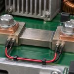
If a power terminal runs hot, don’t replace its thermal relief with a solid connection until you know where the voltage is lost. Under a controlled load, compare the terminal and joint with the pad-to-plane transition and the downstream copper. Only change the relief when the evidence points to that transition, then retest both solder quality and operation.
what is thermal relief in pcb
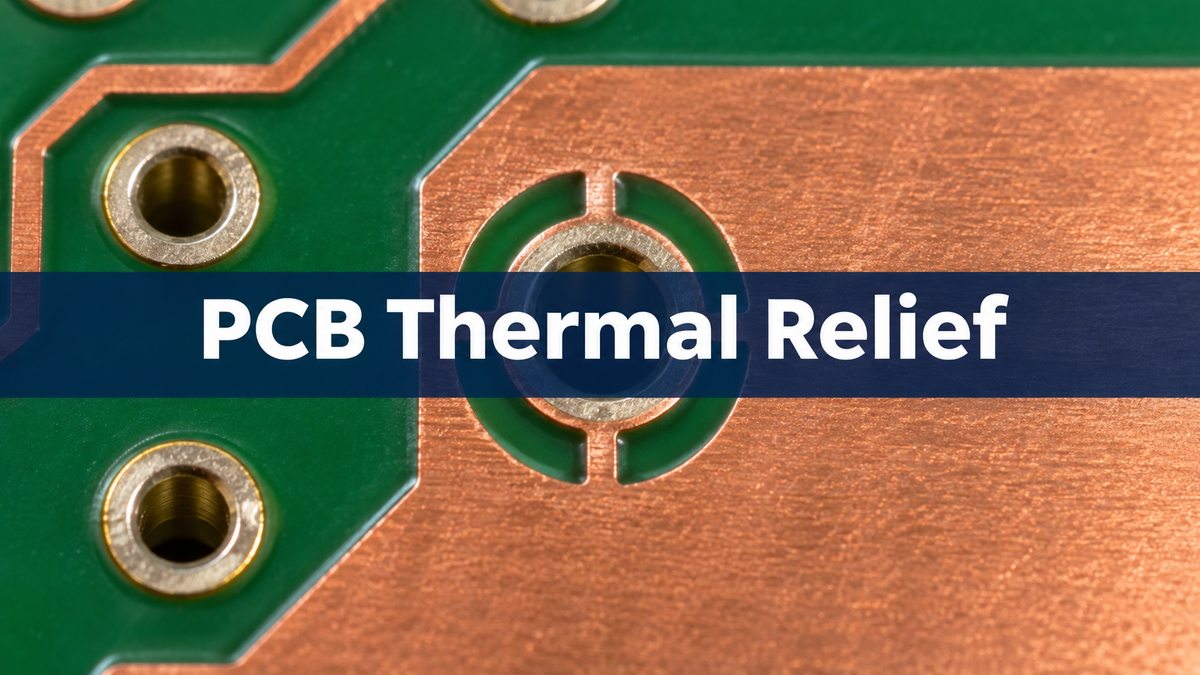
Thermal relief leaves a gap between most of the pad perimeter and its same-net copper plane, with short copper spokes bridging that gap. Less copper cross-section slows heat flow out of the pad while soldering. The same restriction remains in service, so easier soldering and lower operating resistance are separate goals.
thermal relief vs direct connect
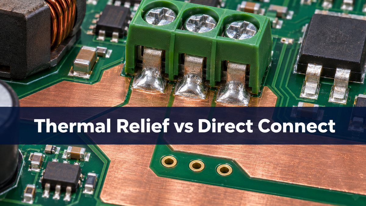
A direct connection is a useful comparison build when the suspect span is the pad-to-plane transition. Keep the connector, copper build and load the same. Changing the connector and the pad in the same trial makes it hard to tell which part of the current path improved. The general thermal relief design guide covers first-pass layout decisions; this article starts with a board that is already running hot.
| Connection | When to consider it | Verify |
| Relief spokes | Plane slows joint heating | Joint, drop and heat |
| Direct copper | Spokes limit current path | Joint and copper neck |
| Revised spoke geometry | Both constraints matter | Actual fill and tests |
thermal relief spoke width
Use finished width, length and copper thickness when estimating a spoke path. Increasing width or adding equivalent spokes can lower its resistance but also lets more heat leave the pad during assembly. In an ideal group of equal spokes, their conductances add in parallel. Real current distribution depends on where the plane is fed, so a layout with four spokes drawn does not necessarily share current evenly.
| Parameter | What to verify |
| Spoke width and length, mm | Finished geometry on each connected layer |
| Remaining spoke count | Connections after zone refill and export |
| Copper thickness, µm | Applicable layer and fabrication build |
| Drop and temperature | Named points and defined load conditions |
pcb thermal relief gap
The relief gap separates the rest of the pad from the plane. A larger gap can lengthen the copper bridge; a nearby clearance can remove a spoke entirely. Refill the zone after a routing change, run the connection checks and inspect the released copper layer. A net name or a schematic check cannot establish what was fabricated.
pcb thermal relief high current
Use the actual operating load and allowable drop to judge the power pad. In a hypothetical 8 A terminal comparison, suppose a four-wire measurement across matched pad-to-plane points gives 3 mΩ for one build and 1 mΩ for another. The corresponding drops are 24 and 8 mV; calculated dissipation in that measured span is 0.192 and 0.064 W. These values are not ratings or measured results. They show why a milliohm-scale restriction can matter.
Plan accessible, named voltage-sense points before energizing the setup. If the board exposes them, use the terminal metal, the PCB pad and the plane just beyond the relief as three successive references. Put the load-current leads outside the sense span. A large terminal-to-pad drop points to the joint and intervening metal; a large pad-to-plane drop points to the PCB transition. If the pin-to-pad boundary is not accessible, report the combined span instead of assigning the loss to the joint. A distant point on the plane can add the loss of an unrelated narrow region.
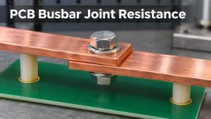
Compare like-for-like at the same load and thermal state. If the hot spot remains but all measured local voltage drops are small, check for a nearby heat source or an unsuitable surface for infrared temperature measurement before blaming the spokes. The busbar joint resistance guide shows the same principle of separating a joint from its conductor.
thermal relief soldering
Check the actual assembly method before treating a solid connection as a defect. A joint that is hard to make by hand may be acceptable under a qualified production process. Conversely, a low-resistance layout is not ready if the joint fails the required inspection. Compare the relief and direct options using representative boards and the intended process; don’t compensate with unapproved soldering conditions.
pcb copper pour
Trace the current from the connector through the pad, spokes or direct entry, layer transitions and the next component. The useful width is the narrowest effective path, not the largest patch of copper in the layout view. Keep unrelated pads on the chosen general rule; apply a documented override only where the individual connection needs it.
pcb thermal relief guidelines
Decide what to change based on the span that failed. For a joint issue, review solder fill and the assembly method. For a PCB transition issue, compare wider spokes or direct copper. For loss downstream, fix the neck or layer transition and leave a sound pad unchanged. Release only after the revised joint, drop and temperature rise meet the agreed limits at the intended load, ambient and enclosure conditions.
FAQ
Are four spokes always better than two?
No. More effective copper can lower resistance, but the result depends on geometry and feeding. It also changes heat flow during soldering.
Does increasing board copper weight fix a missing spoke?
No. First fix or qualify the actual connection. Extra copper cannot replace a segment removed by the pour clearance.
Can I apply the same relief to every ground pad?
Not by default. A signal return, power terminal and heat-dissipating pad may have different connection needs even when they share a net.
Is an exposed package thermal pad the same as thermal relief?
No. A package thermal pad may need to conduct heat away in service. Relief spokes deliberately reduce the copper path around a pad.
Can I use a trace-width calculator as the final acceptance test?
No. It can help screen the layout, but it does not capture every local bottleneck or reproduce the full assembly and load conditions.
Should I measure resistance cold or after loading?
Record both when useful and keep the measurement span fixed. The operating drop and temperature should be checked under the specified load.
Why does my CAD tool report incomplete relief?
A zone rule or nearby clearance can prevent the required number of spokes from connecting. Refill and inspect the actual copper before changing the rule.
Can the same choice be reused after a connector change?
Recheck the pad geometry, copper path, current and assembly conditions. The prior result applies to the tested construction, not automatically to a new footprint.
Sources
KiCad PCB Editor: zone and pad connection settings.
Project Review
For a Best Technology fabrication discussion, send the finished copper thickness, high-current pad geometry, expected load and intended assembly process to sales@bestpcbs.com.
You may also like





Tags: Copper Pour, High Current PCB, PCB Thermal Relief, solderability