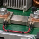
A wide copper pour does not protect a power route if the current must squeeze through a narrow connection at its end. Calculate the neck separately from the rest of the path, then verify temperature on the assembled board. Resistance can be estimated from geometry; temperature also depends on how heat escapes.
What Counts as a Neck-Down?
A neck-down is a local reduction in conductor cross-section. It can occur at a connector pad, fuse land, layer transition, clearance cutout or thermal relief. Follow the actual current path rather than looking only at the largest visible pour.
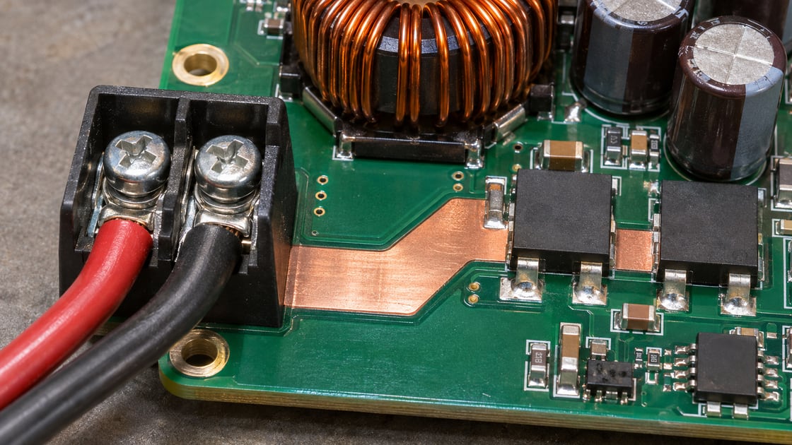
Why the Short Segment Deserves Its Own Calculation
Series segments carry the same steady current, but their resistance per unit length can differ. Texas Instruments’ copper-trace shunt note explains geometry-dependent resistance and the influence of copper temperature. A power connection is not necessarily designed to act as a shunt.
Detailed Inputs for the Resistance Estimate
| Parameter | Example | Purpose |
| — | — | — |
| Steady current | 12 A | Voltage and loss estimate |
| Neck length | 2.0 mm | Defines the segment |
| Finished neck width | 0.60 mm | Sets the cross-section |
| Finished copper thickness | 70 µm | Sets the cross-section |
| Copper resistivity | 0.0172 Ω·mm²/m | Approximate room-temperature input |
Narrow Segment vs Wide Pour
| Section | Example width | Approximate resistance per mm |
| — | — | — |
| Neck | 0.60 mm | 0.410 mΩ |
| Main route | 3.00 mm | 0.082 mΩ |
| Ratio at equal thickness | Five to one in width | Five to one in resistance per length |
Worked Example: Two Millimetres at Twelve Amps
For a rectangular section, R = resistivity × length ÷ area. The neck area is 0.042 mm² and its resistance is about 0.82 mΩ. At 12 A that is about 9.8 mV and 0.118 W. These are hypothetical values before allowing for temperature, contact or current spreading.
Compare the Neck With the Whole Path
A 10 mm length of the 3 mm route has approximately the same ideal resistance as the 2 mm neck. The losses are similar, but one is generated in a much shorter region. Do not infer the same temperature rise; nearby copper, pads and the enclosure can change heat spreading.
Do Not Use Artwork Width as the Only Input
Ask for the relevant finished copper geometry and confirm the narrow section after all clearances and pattern changes. The rectangular approximation becomes less representative where conductor sidewalls slope or the current spreads into a pad.
Compare Widening With a Parallel Route
Widening the neck is straightforward if spacing and soldering constraints allow it. Adding a parallel path can help, but a route that rejoins through the same constriction has not removed it. Verify connection points, vias and current distribution before counting the new copper.
Keep Connector and Joint Heating Separate
A hot terminal can involve the PCB copper, solder joint, contact or wire termination. Measure voltage across the suspected board segment separately where practical. Do not attribute total voltage drop across an assembled connector to the etched trace alone.
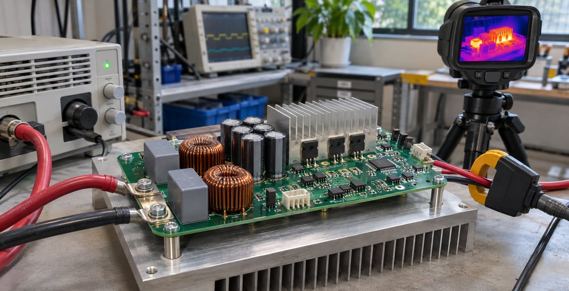
Test the Actual Operating Condition
Use the relevant load, enclosure, airflow and ambient condition. Record duration and the temperature measurement method. With infrared equipment, account for surface emissivity rather than comparing bare shiny copper and dark solder mask without a suitable method.
Check Pulse and Continuous Duty Separately
A short pulse and steady load can create different temperature histories. Calculate electrical loss for the applicable current waveform and verify the thermal response when it matters. Do not apply an illustrative steady-current result as a pulse rating or protection setting.
Carry the Bottleneck Into the Release Review
Mark the narrow section, its finished geometry and the intended verification. The BestPCBs high-current PCB guide covers the wider power-board design. Keep the local calculation linked to the specific pad, connector and drawing revision.
Request a Power Layout Review
Send the current profile and marked bottleneck to Best Technology.
FAQ
Is a two-millimetre neck too short to matter?
Not necessarily. Its importance depends on cross-section, current and the surrounding heat path. Estimate the voltage drop and loss for that segment separately, and compare it with the longer route. If the design is thermally sensitive, check the assembled board under representative conditions.
Can I turn watts directly into temperature rise?
Not without a suitable thermal model or measured relationship for that structure. The same loss can produce different temperatures depending on heat spreading, airflow and nearby materials. Treat electrical power as an input to the thermal problem, not as the final temperature.
Does heavier copper solve every neck-down?
No. Greater thickness may reduce resistance, but it does not remove connector limitations, contact loss, or restrictions from spacing and the fabrication process. Check the finished geometry and follow the current through the pad and any layer transitions before accepting the wider design.
Is a copper pour always better than a trace?
A pour can be useful, but its effective connection can still be limited by a narrow gap, pad entrance or thermal relief. Examine the whole route including the connection points. The largest area of copper is not necessarily the section that determines local loss.
Can I measure the neck resistance with a multimeter?
Very low resistance may be hard to distinguish from lead and contact resistance using an ordinary two-lead setup. Use an appropriate four-terminal measurement or measure voltage drop at a known current where practical. Define the probe points so the result does not include unrelated joints.
Why is the connector hotter than the calculation suggests?
The calculation may describe only the etched copper, while the actual temperature includes heating from the terminal, solder joint or contact resistance. Check the voltage drop of each accessible segment and compare under controlled conditions rather than assigning all the heat to one component.
Should I remove every thermal relief on a power pad?
Not automatically. A solid connection can reduce constriction but can also change assembly heating and solderability. Review the electrical requirement and the assembly process together. If a relief is retained, check the total effective connection and verify the final design under load.
What if two parallel paths have different lengths?
Different lengths and cross-sections can create different resistances, so current need not divide equally. Check the connections, via paths and operating temperature as well as nominal width. Verify each branch if unequal sharing could create a hot spot or exceed a local limit.
You may also like




Tags: copper resistance, High Current PCB, PCB thermal test, PCB trace neck-down