PCB square pad vs round pad compares copper outlines, while the hole shape is a separate feature. A square pad commonly marks Pin 1, while round pads commonly serve the other through-hole pins. The choice still depends on the footprint, pad and hole dimensions, spacing, and assembly conditions. A square pad does not necessarily mean positive polarity, and it is not inherently more reliable.
When you see a square pad, confirm what it identifies before orienting the component. When you build or edit a footprint, decide whether changing the shape helps assembly and whether the finished hole, copper area, and nearby clearances remain suitable.
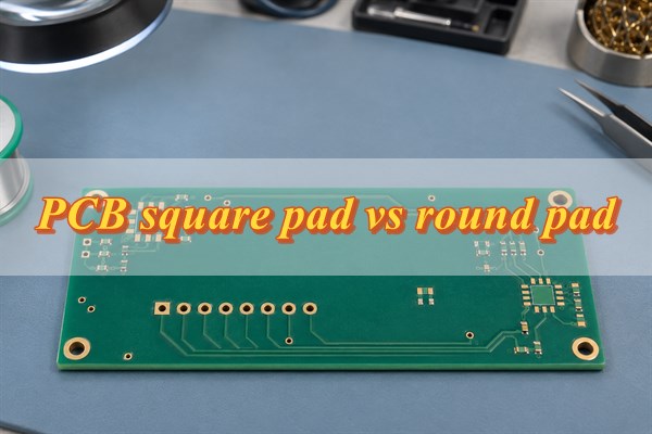
PCB Square Pad vs Round Pad: What Are the Main Differences?
The visible distinction is the copper outline, not necessarily the hole. In the comparison below, both pads are plated through-holes with a centered round hole. Surface-mount lands follow package-specific assembly rules and are outside this through-hole comparison.
| Comparison | Square through-hole pad | Round through-hole pad |
| Copper outline | Four straight sides and four corners | Circular edge at a constant radius |
| Common identification use | Often marks Pin 1 or the footprint starting point | Often used for the remaining pins |
| Copper at the same outer width | Greater outline area because the corners add copper | Smaller outline area within the same diameter |
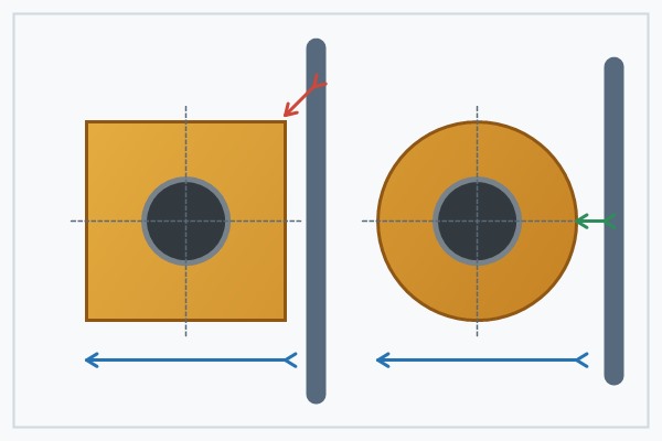
| Clearance envelope | Corners reach farther diagonally from the center | Boundary is equally distant from the center in every direction |
| Typical reason to choose it | Visual Pin 1 cue when the footprint convention requires it | Consistent geometry when a special pin marker is unnecessary |
These are conventions and geometric consequences, not automatic electrical properties. At the same outer width and hole size, the square occupies more area at its corners; at the same copper area, the two pads have different outer dimensions. A valid comparison must state which condition is held constant.
Pad shape does not determine drill shape. Most square through-hole copper pads surround round plated holes. EDA tools store the land, hole, mask opening, and plane connection as separate footprint features.
Why Do PCBs Often Use a Square Pad for Pin 1?
A square pad gives designers, assemblers, and repair technicians a quick visual reference for the beginning of a pin sequence. On a single-row through-hole header, for example, the square land can identify Pin 1 while Pins 2 through 8 remain round. On a DIP footprint, it can reinforce the package notch, dot, silkscreen outline, and assembly drawing rather than replace them.
This practice is a common footprint-library convention because the shape remains visible in PCB artwork and can be recognized even when a reference designator is hard to read. It also helps when comparing the physical board with a schematic symbol or connector pinout. The convention is useful only when the footprint pad number, schematic pin number, and component drawing all agree.
The square is an orientation cue, not independent proof of pin numbering. A custom or legacy library may use another marker, and some non-polarized footprints use identical pad shapes. Confirm Pin 1 against controlled design data before assembly or rework.
Does a Square PCB Pad Always Indicate Positive Polarity?
No. Pin number and electrical polarity describe different things. Pin 1 may be a supply input, ground, signal, enable pin, shield connection, or another function, depending on the component definition; a square pad identifies the numbered position only when the footprint convention says it does.
Confirm polarity by tracing the component data sheet through the schematic to the footprint pad numbers. Check the silkscreen, assembly drawing, and the component’s molded, printed, notched, or banded mark. These sources should indicate the same installed direction.
Consider a polarized radial capacitor in a footprint whose square pad marks Pin 1. That pin could be assigned to the positive lead in one verified library, but the square cannot establish that assignment by itself. If the symbol-to-footprint mapping or library convention differs, using shape alone could reverse the component even though the land pattern looks familiar.
How Does Pad Shape Affect Copper Area and Clearance?
Pad shape changes the copper envelope when the comparison uses the same outer width and the same centered hole. Let the square side and circle diameter both be D, and let the round-hole diameter be d. The square outline area is D2, while the circular outline area is pi × D2/4; the hole removes pi × d2/4 from either ideal outline.
Geometric illustration only: suppose D is 2.0 mm and d is 1.0 mm. These values are chosen to make the arithmetic clear, not to recommend a pad or finished-hole size.
| Ideal two-dimensional result | Square pad | Round pad |
| Outer copper area | 4.00 mm2 | 3.14 mm2 |
| Round-hole area | 0.79 mm2 | 0.79 mm2 |
| Copper remaining after subtracting the hole | 3.21 mm2 | 2.36 mm2 |
| Farthest reach from pad center | 1.41 mm at a corner | 1.00 mm at the circular edge |
Although the square has about 0.86 mm2 more copper in this ideal view, both shapes have the same nominal ring at the square’s flat side or the circle’s edge: (D – d)/2, or 0.50 mm before manufacturing tolerances. The extra corner copper does not increase that narrowest ring. It does not, by itself, prove a stronger joint, higher current rating, better heat transfer, or greater field reliability.
Clearance can move in the opposite direction. The square corner extends roughly 0.41 mm farther from center in this example, leaving less space for a diagonal trace, pad, pour, or board edge. If equal copper area is the target, recalculate clearance from the new envelopes rather than reusing the equal-width result.
PCB Square Pad vs Round Pad: How Does Soldering Differ?
For comparable through-hole joints, outer shape is only one soldering condition. Finished-hole fit, lead geometry, pad size, finish, flux, preheat, heat input, dwell time, and joint access can matter more. A square outline cannot compensate for a tight hole, undersized ring, or unsuitable process window.
The copper connected beyond the pad is especially important. Imagine the same through-hole connector with one round pad tied directly to a large ground plane and one square pad connected through an effective thermal relief. The round pad may require more heat because the plane removes energy from the joint, even though someone comparing shape alone might predict the opposite. Reversing the plane connections could reverse the observed behavior.
Separate wetting on the visible land from solder fill inside the plated barrel. Land geometry affects the exposed surface and local solder-mask boundary, while barrel fill depends on hole-to-lead fit, plating, thermal balance, solder delivery, and process control. Square corners do not inevitably create a soldering defect, and a round outline does not guarantee complete fill or a reliable connection.
PCB Square Pad vs Round Pad: When Should You Use Each?
Use shape as a controlled footprint decision. A square pad is valuable when a clear Pin 1 cue helps placement or inspection and the corner envelope still meets spacing rules. Round pads are appropriate for the other pins or for a footprint in which every pin may use the same shape without losing necessary orientation information.
| Design condition | Preferred action | Reason to verify |
| Pin 1 needs a visible board-level cue | Use a square pad for Pin 1 and round pads for the remaining pins | Confirm the cue agrees with the symbol, footprint numbering, and component drawing |
| The part is non-polarized and pin distinction is unnecessary | Round pads may be used throughout | Check that assembly and test documentation do not rely on a special marker |
| Available diagonal space is limited | Evaluate a round pad or resize the approved land pattern | Check annular ring and copper clearance after every change |
| A manufacturer footprint or validated library already exists | Follow it unless a documented design need justifies a revision | Revalidate numbering, dimensions, mask, courtyard, and assembly evidence if modified |
An oval or rounded rectangle may solve a specific lead or spacing problem, but it should not be added for visual variety. Follow the component land pattern, controlled library convention, available space, and confirmed fabrication and assembly capabilities.
Changing one pad in a verified footprint can alter clearance, solder-mask webs, copper-pour behavior, thermal connections, and automated checks. Preserve the original revision, document the reason, and rerun the relevant electrical, DFM, and assembly checks.
How Should You Size Square and Round Through-Hole Pads?
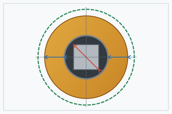
Start with maximum lead dimensions, not a typical value. Compare a round lead’s maximum diameter with the finished-hole range. For a square lead in a round hole, check the maximum corner-to-corner dimension: a sharp square of side a has diagonal a√2. Rounded corners, chamfers, plating, or a rectangular section change the actual envelope.
Set the finished hole from lead variation, insertion allowance, plating, drill behavior, and assembly method. A wave-soldered connector, a hand-inserted component, and a press-fit contact do not share one clearance rule. Press-fit systems require the connector manufacturer’s hole and plating specification.
Size the land from the required finished annular ring and the fabricator’s tolerances. For a centered round hole, pad width = finished-hole diameter + 2 × nominal ring is a starting relationship. Choose the nominal ring so the narrowest finished copper still passes after drill offset, hole-size variation, etch effects, and applicable standards.
The square pad’s corners add area but do not replace copper at the flat sides, its narrowest locations around a round hole. Check those sides for annular-ring compliance, then check the corners against neighboring pads, traces, planes, slots, and the board edge. A round pad uses the same radial clearance in every direction, but it still needs a tolerance-aware clearance check.
Set the solder-mask opening and assembly conditions as independent constraints. The opening must expose the intended land without eliminating a required mask web or creating an unreviewed bridge between close pads. Confirm whether the fabricator uses specified mask expansion, adjusted production data, or other documented rules, and verify that inspection and solder access remain practical for the selected process.
What Pad Design Checks Are Needed Before PCB Manufacturing?
Run the checks on the released footprint and manufacturing outputs, not on an earlier library preview. Before manufacturing, review the final PCB square pad vs round pad choice against the same component installation, numbering, physical fit, and output data.
- Pin identity: match the data-sheet pin numbers to the schematic symbol, footprint pad numbers, and assembly drawing.
- Polarity evidence: compare the component body mark, silkscreen, assembly notation, and electrical assignment instead of inferring polarity from pad shape.
- Finished-hole fit: check maximum lead dimensions, including the diagonal of square or rectangular pins, against the specified finished-hole range and insertion method.
- Annular ring: verify the narrowest finished ring after relevant hole, registration, and copper tolerances.
- Copper clearance: measure square-pad corners and all nearby traces, pours, pads, slots, and board edges using the applicable production rules.
- Solder mask and assembly: review mask openings, mask webs, thermal reliefs, plane connections, solder access, and inspection needs.
- Output consistency: confirm the Gerber or other copper data, drill file, fabrication notes, BOM, pick-and-place data where applicable, and assembly drawing use the same footprint revision and orientation.
EBest Circuit can review the pad, hole, clearance, mask, and assembly conditions against the intended manufacturing process. For a DFM review, send the Gerber files, drill files, BOM, and assembly drawing to sales@bestpcbs.com, along with the component data sheet when lead dimensions or pin orientation need confirmation.
FAQs About PCB Square Pad vs Round Pad
Q1: Can a mechanical mounting pin use a square copper pad?
A1: Yes, when the land pattern calls for copper. Some retention or shield pins need a plated copper land, while a purely mechanical feature may use a non-plated hole with no copper. Follow the component drawing; a square outline does not improve retention by itself.
Q2: Can one through-hole pad use different copper shapes on different layers?
A2: Yes, in pad-stack systems that support layer-specific geometry. Use different shapes only for a documented electrical or manufacturing purpose, then inspect every copper layer together with the drill data before release.
Q3: Must the Pin 1 copper marker remain visible after component placement?
A3: Not necessarily. The marker must help orient the part before insertion, but a component body may cover it afterward. If inspection or rework needs a visible reference, add a matching external cue on the silkscreen or assembly drawing.
Q4: Will the solder-mask opening always preserve a square pad outline?
A4: No. Mask expansion, a separately defined mask shape, a merged opening, or tenting can change what remains visible. Check the actual solder-mask output if operators are expected to use the square outline as a Pin 1 cue.
Q5: Can a through-hole pad also serve as a test point?
A5: Yes, if it meets the test requirements. Confirm the probe side, accessible contact area, surface finish, clearance, mechanical support, and expected contact cycles. The pad’s square or round outline is secondary to reliable probe access.
Q6: Should one pad-shape convention be used across the whole PCB?
A6: Usually, because consistency reduces interpretation errors. A manufacturer-recommended or verified library footprint may justify an exception. Document it and keep the schematic, footprint, assembly drawing, and test documentation aligned.
You may also like



Tags: DFM Review, PCB Copper Pad, pcb footprint, Plated Through Hole, through hole soldering