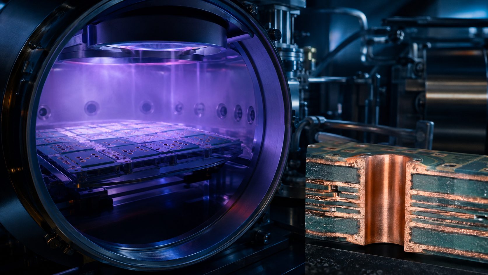
PCB plasma desmear uses a controlled low-pressure plasma to remove organic drilling smear and condition hole walls before electroless copper and plating. It is especially useful where mechanical drilling or laser processing leaves polymer residue that can block a reliable connection to exposed inner-layer copper.
Plasma is not automatically better than a chemical desmear for every board. The correct route depends on laminate chemistry, hole type, aspect ratio, layer structure, required etchback and the fabricator’s qualified process. Buyers should ask how the selected process is controlled and verified for their exact construction.
What PCB Plasma Desmear Removes
Plasma desmear primarily removes carbon-based resin residue from drilled or laser-formed hole walls. Mechanical drilling can heat and smear resin across exposed copper. Laser ablation can leave organic residue or redeposited material inside microvias. If that layer remains, subsequent metallization may not form a consistent electrical interface.
The process can also modify the polymer surface to improve wetting and adhesion for the next manufacturing stages. It does not replace every cleaning, conditioning or metallization step, and it cannot repair a badly positioned drill, damaged inner-layer pad or incorrect stackup.
Why Drill Smear Blocks a Reliable Inner-Layer Connection
Smear can act as an insulating film between the plated barrel and the inner-layer copper. A finished hole may look continuous from the surface while the buried junction remains weak or open. Thermal cycling can further expose an incomplete connection.
The risk is not determined by visible residue alone. Engineers should evaluate the actual inner-layer junction, copper coverage and interconnect continuity. For a broader view of the finished structure, see our plated through-hole PCB guide.
How the Plasma Desmear Process Works
- Load panels or coupons in a fixture that allows gas access to the relevant holes.
- Evacuate the chamber to the controlled process pressure.
- Introduce the qualified process gases.
- Apply radio-frequency energy to create reactive plasma species.
- Allow the plasma to react with exposed organic residue.
- Remove volatile reaction products through the vacuum system.
- Complete any required conditioning and metallization route.
- Verify the result with process coupons, microsections or other agreed evidence.
Recipe time, gas balance, pressure, power, loading and fixture geometry interact. A recipe qualified for one laminate or hole geometry should not be assumed suitable for another.
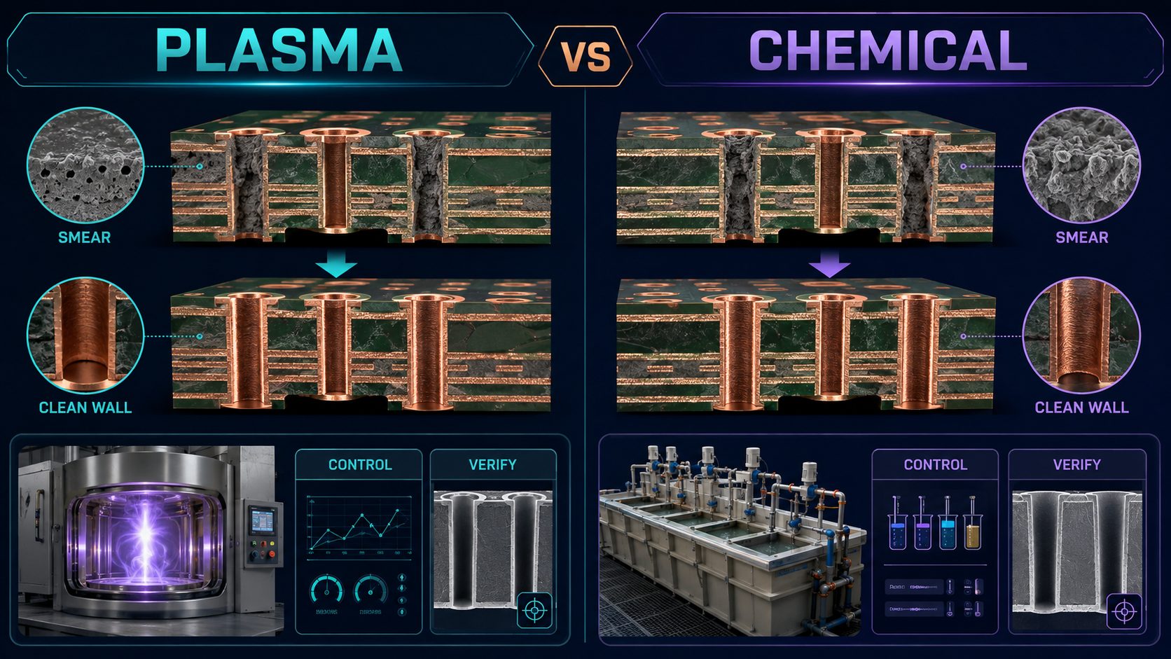
Plasma Desmear vs Permanganate Chemical Desmear
| Decision point | Plasma route | Chemical route |
| Removal mechanism | Gas-phase reaction with organic residue | Wet chemical oxidation and conditioning |
| Material fit | Useful for selected high-performance resins and small features when qualified | Established for many conventional multilayer constructions |
| Access | Depends on chamber loading and gas transport into holes | Depends on solution exchange and wetting |
| Process control | Power, pressure, gas, time and load geometry | Concentration, temperature, dwell, agitation and bath loading |
| Verification | Hole-wall/junction evidence on representative samples | Hole-wall/junction evidence on representative samples |
Where Plasma Treatment Is Most Useful
Plasma becomes valuable when the material system, feature geometry or residue is not well served by the standard wet route. Potential applications include selected high-performance laminates, PTFE-containing constructions, flex materials, small laser vias and hybrid stackups. Suitability still requires fabrication review and qualification.
- Confirm every dielectric material and adhesive in the stackup.
- Separate mechanically drilled holes from laser microvias.
- Identify the smallest, deepest and most difficult-to-access features.
- Define whether desmear, etchback or surface activation is required.
- Review material-supplier processing guidance where available.
- Use representative coupons rather than a simpler substitute construction.
For microvia structure decisions, refer to the HDI PCB fabrication guide.
Process Inputs That Must Be Controlled
A repeatable plasma result depends on controlled inputs, load configuration and equipment condition.
- verified material and stackup revision;
- hole type, depth, diameter and panel thickness;
- preclean and drying condition;
- gas identity, flow and mixture;
- chamber pressure, power and exposure time;
- panel spacing, orientation and batch loading;
- electrode/chamber cleanliness and maintenance;
- recipe revision, operator and lot traceability;
- time and handling before downstream metallization.
Monitor actual process records, not only the programmed recipe. A load that shields holes or changes gas distribution can fail even when the screen shows the expected settings.
Need a desmear route reviewed for your stackup?
Send the controlled stackup, material designations, drill files, via structures and inspection requirement. EBest Circuit can review whether plasma, chemical desmear or a qualified combination should be discussed before quotation.
Signs of Under-Desmear and Over-Treatment
| Condition | Possible evidence | Next check |
| Under-desmear | Residual smear, incomplete inner-layer copper exposure or weak metallization interface | Recipe/load access and preclean condition |
| Nonuniform treatment | Panel-position or hole-orientation variation | Fixture, loading, chamber uniformity and sample map |
| Over-treatment | Excessive resin removal, glass exposure or altered hole geometry | Exposure severity and material compatibility |
| Downstream issue | Clean wall but plating void or poor coverage | Conditioning, activation and metallization controls |
| Preparation artifact | Apparent residue or relief changes between sections | Repeat specimen preparation |
A clean-looking wall does not prove the full plated connection is acceptable. Review the junction after downstream processing and distinguish desmear evidence from plating evidence.
How to Qualify Plasma Desmear for a PCB Construction
- Freeze the representative stackup, materials and hole structures.
- Define the defect or residue that the process must remove.
- Select worst-case features and panel locations.
- Run a controlled recipe window with traceable loads.
- Inspect hole walls and inner-layer junctions before and after metallization.
- Apply any required thermal or reliability conditioning.
- Compare electrical and cross-sectional evidence with acceptance requirements.
- Document the approved recipe, load limits, controls and requalification triggers.
Requalification may be needed after material, stackup, hole geometry, equipment, recipe or loading changes. The trigger should be defined in the control plan rather than decided after a failure.
Microsection and Hole-Wall Evidence to Review
Microsection evidence should show the full feature and the critical junctions at useful magnification. Record sample identity, panel position, hole type, orientation, preparation condition and whether the specimen was thermally stressed.
- remaining smear or organic residue;
- inner-layer copper exposure and junction condition;
- resin and glass morphology;
- barrel coverage and plating continuity;
- voids, separation, cracks or over-etchback;
- comparison across panel positions and process loads.
Use our PCB microsection analysis guide to structure the report. If a copper/dielectric gap is present, also review the hole wall pullaway guide rather than labeling every junction anomaly as smear.
Design and Stackup Information the Fabricator Needs
- Gerber or ODB++ and released fabrication drawing;
- complete material and adhesive designations;
- controlled stackup and copper weights;
- NC drill and laser data with hole groups;
- finished dimensions and layer connections;
- special desmear or etchback requirement;
- acceptance class and customer-specific criteria;
- coupon, microsection and thermal-test requirements;
- quantity, revision, delivery and traceability needs.
A fabrication note that only says “plasma required” is incomplete. State why it is required and allow the fabricator to confirm the qualified route for the actual construction.
Cost and Lead-Time Questions for an RFQ
Plasma cost is influenced by qualification, batch loading, material route, inspection and whether the process is standard for the construction. Ask:
- Is plasma already qualified for every specified material?
- Is a trial or coupon build required?
- Which hole groups receive the treatment?
- What inspection and report are included?
- What changes would trigger requalification?
- Does the route add handling, queue or outsourced-process time?
- How are loads and recipe revisions traced?
Quote the process and evidence together
Include material, stackup, hole groups, quantities and required inspection. That allows the manufacturing route, qualification effort and lead-time impact to be evaluated before release.
FAQ About PCB Plasma Desmear
What is smear in a drilled PCB hole?
It is resin residue displaced or redeposited on the hole wall, potentially covering exposed inner-layer copper.
Does plasma desmear replace electroless copper?
No. It prepares the hole wall; metallization and electroplating are separate downstream processes.
Is plasma required for every multilayer PCB?
No. Many constructions use qualified wet chemical desmear. Selection depends on materials, geometry and the fabricator’s validated route.
Can plasma be used for microvias?
It can be useful for selected laser-via constructions, but gas access, material compatibility and qualification must be confirmed.
Is plasma always better for PTFE materials?
No universal rule applies. The exact PTFE-containing material, surface treatment and downstream process determine the route.
Can too much plasma damage a hole wall?
Excessive treatment can change resin/glass morphology or geometry, so the recipe needs a controlled window.
How is desmear effectiveness inspected?
Representative microsections can show residue removal, inner-layer exposure and the plated junction; process coupons and electrical/reliability evidence may also apply.
What is the difference between desmear and etchback?
Desmear targets drilling residue. Etchback intentionally removes dielectric to expose more inner-layer copper; requirements should be stated separately.
What should be included on the drawing?
Identify materials, hole groups, relevant treatment intent, acceptance criteria and required coupon or inspection evidence.
What proves the process is controlled?
Approved recipes, actual load records, maintenance, traceability and representative verification evidence together provide stronger proof than a generic equipment claim.
Final Process-Selection Checklist
- Identify the actual smear/residue and hole type.
- Confirm every dielectric and adhesive material.
- Compare plasma and chemical routes for the construction.
- Define load, recipe and maintenance controls.
- Inspect inner-layer junctions after downstream metallization.
- Qualify worst-case features and panel positions.
- Document requalification triggers.
- Include process and evidence requirements in the RFQ.
Request a construction-specific PCB process review.
Send Gerber or ODB++, stackup, material designations, drill/laser data, inspection criteria, quantity and delivery target to sales@bestpcbs.com, or use the PCB quote form. EBest Circuit will review the manufacturing route and identify any qualification evidence needed before production.
You may also like



Tags: pcb manufacturing process, PCB Quality Control, Plated Through Hole