





Choosing among HDI PCB manufacturers in UK requires more than finding a supplier that lists “HDI” on a capability page. The right manufacturer must review your actual buildup, explain how each microvia is formed and filled, identify the proposed production site, and show how the released construction will be controlled from prototype through repeat orders.
Start with the features that create manufacturing risk: microvia layer pairs, stacked or staggered structures, via-in-pad, lamination cycles, finished copper, fine features, material system and impedance requirements. Then compare suppliers using the same files, quantities, inspection scope and delivery assumptions. This exposes incomplete quotations early and turns a general supplier search into a defensible manufacturing decision.

How to Choose an HDI PCB Manufacturer in UK?
Choose an HDI PCB manufacturer in UK by matching the proposed factory, process controls and evidence package to your board. A UK address may represent a fabrication site, sales office, managed supply service or assembly provider, so the quotation should name where the bare board will be produced and which operations are subcontracted.
- Match the buildup: submit the layer stack and microvia start/stop layers so the supplier cannot silently simplify the routing concept.
- Confirm materials: identify the laminate family, electrical properties and acceptable substitutions because changes can alter impedance and pressing behavior.
- Check prototype and production routes: ask whether both use the same site, materials and critical processes; define approval for any transfer.
- Agree on evidence: specify electrical test, microsection, impedance verification, inspection reports and lot records before comparing prices.
- Evaluate assembly ownership: for BGA, CSP or via-in-pad designs, determine how bare-board findings return to the assembly team.
- Judge communication by output: a useful supplier returns a marked-up stackup, DFM questions, deviations and an evidence plan—not only a quick reply.
What Capabilities Should HDI PCB Manufacturers in UK Provide?
Look for capabilities that correspond directly to routing, component, signal-integrity and reliability requirements. Minimums depend on layer count, copper weight, material, panel size and volume.
| HDI process capability | Published UK capability example |
|---|---|
| Maximum layer count | Up to 32 layers |
| Laser microvia diameter | Down to 75 µm |
| Mechanical drill diameter | Down to 0.105 mm |
| Fine track and gap | Down to 50 µm |
| Microvia aspect ratio | Up to 1:1 |
| Sequential lamination | Up to 6 lamination cycles |
| Supported via structures | Blind, buried, stacked and staggered microvias |
| Via filling | Copper-filled and resin-filled vias |
| Controlled impedance | ±10% standard; ±5% advanced capability |
| Electrical test | 100% electrical test |
The numerical examples above are currently published by Exception PCB for its UK HDI production environment; Rush PCB UK separately publishes up to 20+ layers, 0.1 mm microvias and 50/50 µm trace/space. These are screening references, not universal limits for all HDI PCB manufacturers in UK. Require the shortlisted factory to return values tied to your material, copper, panel and volume.
How Can You Verify a Reliable HDI PCB Manufacturer in UK?
A reliable manufacturer connects each important claim to a site-specific process, review record and acceptance method. Certificates may support qualification, but they do not prove that a particular microvia stack has been assessed.
- Build-specific DFM: require comments tied to actual layer pairs, microvia spans, copper, materials and tolerances. A generic “approved” response does not show that the construction was reviewed.
- Named production site: record the physical factory and which processes it performs. If laser drilling, filling or testing is subcontracted, require the responsible site and control method.
- Material traceability: record manufacturer, grade and lot identity, and require approval before substitution. This protects impedance and lamination behavior from unreviewed changes.
- Microvia evidence: agree on microsection locations, plating and fill criteria, sampling frequency and the report supplied with the order.
- Electrical and impedance testing: define the source netlist, test coverage, coupon design, target tolerance and report format rather than accepting “tested” as a complete answer.
- Registration control: ask how sequential-lamination registration is monitored and what evidence demonstrates that capture pads and interlayer alignment meet the drawing.
- Prototype-to-production consistency: confirm whether the same stackup, material, factory and critical process route will be used after prototype approval.
- Change and nonconformance control: define which changes need written approval and who owns containment, root-cause analysis and corrective action after fabrication or assembly.
Request report samples before ordering. This proves the evidence is part of the operating process rather than a document requested after the boards are finished.
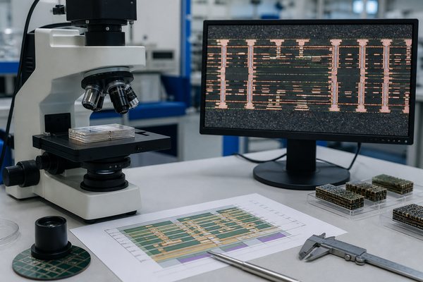
Why Choose EBest as an Alternative to HDI PCB Manufacturers in UK?
When UK production is not a contractual requirement, EBest Circuit offers a China-based route that connects HDI fabrication, engineering review and PCB assembly. EBest is not presented as a UK manufacturer; it is an alternative for UK projects needing coordinated overseas manufacturing.
- Build-specific review: stackup, microvia map, via-in-pad, materials and impedance are reviewed against the intended construction.
- DFM before production: Gerber or ODB++, drill data and notes are checked for ambiguous transitions, conflicts and avoidable complexity.
- Fabrication and assembly coordination: board production, sourcing, SMT, inspection and test can share one project workflow.
- Prototype-to-volume control: approved data, revisions and deviations can be retained for later builds.
- Project-defined evidence: electrical test, AOI, microsection, impedance and assembly inspection are scoped to the design.
- Pre-quotation support: unresolved manufacturing and assembly questions are identified before commercial comparison.
Send Gerber or ODB++, stackup, drill files and project requirements to sales@bestpcbs.com for a free DFM review and quotation.
How Should You Compare Quotes From HDI PCB Manufacturers in UK?
Compare quotations only after every HDI PCB manufacturer in UK has priced the same construction, production route and acceptance evidence. Use the following checks:
- Freeze the technical baseline: use one released stackup, via map, material requirement, copper weight, surface finish and impedance table. Otherwise, a lower quote may represent a simpler board.
- Separate setup from unit price: identify tooling, engineering, coupons and one-time test charges so repeat-order cost is visible.
- Confirm the buildup assumption: require the quoted lamination cycles and stacked/staggered microvia treatment in writing because they are major cost drivers.
- Check included evidence: state whether electrical test, impedance reports, microsections, first-article records and certificates are included or charged separately.
- Identify the production site: compare UK-built, UK-managed and overseas manufacture honestly; include freight, import handling and any transfer risk.
- Normalize quantity and delivery: request the same prototype, pilot and repeat-order quantities with the same delivery point and required date.
- List every deviation: a quote that substitutes material or omits a process is not comparable until the difference is reviewed and accepted.
Which Design Choices Increase Quotes From HDI PCB Manufacturers in UK?
Design choices increase cost when they add process cycles, reduce yield or require tighter verification. DFM can reduce those costs without weakening function.
- Extra buildup cycles: each adds pressing, drilling, imaging and registration work.
- Stacked microvias: use them for necessary vertical transitions; staggered structures may be simpler when routing permits.
- Filled and capped vias: restrict them to locations that require pad escape, thermal or assembly performance.
- Fine features: review local bottlenecks instead of applying an extreme rule across the board.
- Specialty materials: specify performance needs and permitted alternatives to avoid unnecessary sourcing constraints.
- Inspection: connect each extra record or test to a real risk and acceptance decision.
What Lead Time Should You Expect From an HDI PCB Manufacturer in UK?
Published UK supplier examples place HDI prototypes from about 5 working days, while more complex HDI/BBV builds are commonly presented around 7–10 working days. Some suppliers advertise 1–5-day expedited options, but those are conditional services rather than a dependable default for every stackup.
| Planning case | Indicative published range | What can extend it |
|---|---|---|
| Simple, materials-available HDI prototype | From about 5 working days | Open DFM questions, special material, via filling or added reports |
| More complex HDI or blind/buried-via build | About 7–10 working days as a planning reference | Multiple lamination cycles, stacked vias, tight registration or non-stock laminate |
| Expedited service | Some UK suppliers advertise 1–5 working days | Available only after design, material, capacity and inspection review |
| HDI plus assembly | Bare-board lead time plus component and PCBA schedule | Long-lead components, stencil, programming, X-ray or functional testing |
The ranges are based on current supplier-published examples: Pure PCB lists HDI prototypes from five working days and an HDI/BBV range of 7–10 days, while Rush PCB UK advertises conditional 1–5-day quick-turn options. Treat them as RFQ planning references, not EBest promises or universal UK lead times. Ask the selected manufacturer to return a milestone schedule covering DFM approval, material release, lamination, drilling/filling, inspection, assembly and shipping.
How Should an HDI PCB Manufacturer in UK Select Materials?
An HDI PCB manufacturer in UK should select a material system from the electrical requirement, thermal exposure, lamination sequence, thickness target and supply risk—not from Tg alone.
- For standard digital and industrial HDI: confirm that the chosen high-Tg FR-4 supports the required press cycles and finished thickness without uncontrolled material substitution.
- For high-speed or RF nets: provide target Dk/Df assumptions, frequency and impedance geometry so the fabricator can model the actual construction.
- For repeated reflow or higher thermal demand: review decomposition behavior, z-axis expansion and moisture control together with the assembly profile.
- For thin dielectrics and microvias: verify that prepreg and core availability supports the required microvia depth, resin flow and copper distribution.
- For procurement continuity: name the preferred grade and approved equivalent criteria; require notification before any change that affects impedance or lamination.
The RFQ should record manufacturer, grade, dielectric construction, copper type and weight, required electrical data, approved alternatives and substitution authority. The reviewed production stackup should be returned before release.
How Should an HDI PCB Manufacturer in UK Control Via-in-Pad?
An HDI PCB manufacturer in UK should control via-in-pad as a complete fill, cap and surface-planarity process. The buyer should verify:
- Via geometry: define drill diameter, depth, aspect ratio and connected layers so the fill process is evaluated against the real structure.
- Fill and cap: state whether conductive or non-conductive fill is required, the copper-cap expectation and any void acceptance criterion.
- Planarity: specify the finished BGA/CSP pad requirement and inspection method because uneven pads can change paste volume and joint formation.
- Surface finish: review finish selection and thickness after planarization; the final pad, not the unprocessed via, must meet assembly needs.
- Fabrication-to-PCBA feedback: align stencil, reflow and X-ray inspection with pad acceptance so solder defects can be separated from bare-board defects.
Put these requirements in the fabrication drawing and via map. Do not rely on a note that says only “VIPPO” or “via-in-pad,” because it does not define the acceptance result.
How Should an HDI PCB Manufacturer in UK Plan Sequential Lamination?
An HDI PCB manufacturer in UK should translate the via map into a documented sequence of core preparation, lamination, laser drilling, filling and inspection.
- Map every microvia span: show which vias are formed after each press cycle and where stacked interfaces occur.
- Confirm the minimum necessary cycles: extra buildup stages increase alignment work, cost and lead time; remove a cycle when routing permits a simpler transition.
- Control materials through repeated pressing: verify dielectric thickness, resin behavior and copper balance for the complete thermal history.
- Protect registration: review capture pads, material movement allowances and the evidence used to verify interlayer alignment.
- Define stage-specific inspection: identify which structures require microsection or other checks before later layers make them inaccessible.
- Freeze the production stackup: require approval before changing layer sequence, material, site or via structure after prototype acceptance.
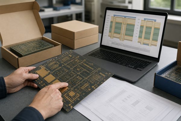
What Files Should You Send to an HDI PCB Manufacturer in UK?
A useful quote needs enough released data to identify the actual process route. Send the same package to each supplier.
- Gerber or ODB++: release the copper, mask, legend and profile geometry from one controlled revision.
- NC drill and microvia map: distinguish mechanical, buried, blind and laser-drilled holes and show every start/stop layer.
- Production stackup: define the buildup, dielectric thicknesses, copper weights, material grades and finished thickness.
- Fabrication drawing: state finished-hole rules, via fill/cap, surface finish, tolerances and special acceptance notes.
- Impedance table: identify nets, layers, target, tolerance, reference planes and required reporting.
- Quantity schedule: separate prototype, pilot and repeat volumes so tooling, panelization and unit pricing can be compared.
- PCBA data when required: include BOM, pick-and-place, assembly drawing, approved substitutions and component-sourcing scope.
- Inspection and test requirements: define electrical test, microsection, impedance, X-ray, programming and functional-test deliverables as applicable.
- Commercial inputs: provide delivery destination, required date, Incoterm request and any country-of-manufacture restriction.
Also state prototype and repeat quantities, destination, origin constraints and required records. Ask for a reviewed stackup, deviations, proposed site and included inspection scope.
Submit the complete package with the RFQ and request an HDI DFM review covering both fabrication and assembly requirements.
How Should HDI PCB Manufacturers in UK Prevent Common Defects?
Prevent the main HDI defects by controlling the design input, process window and inspection point for each risk:
- Microvia interconnect failure: keep the via diameter, depth and aspect ratio inside the approved process window; control laser drilling, interface preparation and plating; verify critical structures by electrical test and targeted microsection.
- Incomplete via fill: match copper or resin fill to the via geometry, define acceptable voiding and inspect the filled structure before later processing hides it.
- Poor via-in-pad planarity: specify fill, cap-plating and finished-pad requirements; inspect the surface before assembly to prevent solder wicking and inconsistent joints.
- Layer misregistration: provide adequate capture pads, account for material movement and check alignment after each relevant lamination stage rather than only at final inspection.
- Delamination: use a compatible material system, control moisture and contamination, and validate the press and thermal history for repeated lamination and reflow.
- Impedance deviation: freeze dielectric thickness, copper geometry and material data in the production stackup; measure agreed coupons against the stated tolerance.
- Open or short circuits: run 100% electrical testing against the correct released netlist and keep repair or concession records tied to the lot.
- Prototype-to-volume drift: prevent unapproved changes to the factory, material, stackup, via treatment and inspection plan after the prototype is accepted.
FAQs About HDI PCB Manufacturers in UK
Q1: Are HDI PCBs always more expensive than standard multilayer PCBs?
A1: They usually involve additional processes, but the difference depends on buildup, microvias, materials, testing and quantity.
Q2: What is the minimum layer count for an HDI PCB?
A2: Layer count alone does not define HDI; high-density interconnection methods do.
Q3: Are stacked microvias better than staggered microvias?
A3: Neither is universally better. Select the structure from routing need and manufacturing risk.
Q4: Can HDI PCBs use controlled impedance?
A4: Yes. Provide target, tolerance, geometry and material assumptions and agree on coupon reporting.
Q5: Which surface finish suits fine-pitch HDI assembly?
A5: Choose it from pad geometry, assembly, storage and reliability needs, then review planarity with the assembler.
Q6: Do all microvias need to be filled?
A6: No. Filling depends on structure and use; via-in-pad and some stacked configurations need a defined fill and cap.
Q7: Should prototype and volume boards use the same stackup?
A7: The prototype should represent production where possible; later changes may require review or requalification.
Q8: Is DFM review necessary before production?
A8: Yes. It can find conflicting via structures, unsupported rules and incomplete acceptance criteria.
Q9: Can HDI boards use fine-pitch BGA and CSP packages?
A9: Yes, when pads, via treatment, finish, stencil, reflow and inspection are coordinated.
Q10: How should UK and overseas suppliers be compared?
A10: Use identical files, quantities, evidence, assembly scope, destination and change controls, then compare total responsibility and risk.
Conclusion
The right supplier turns a released HDI design into a controlled, inspectable and repeatable manufacturing plan. Confirm the build site, match capabilities to the stackup, require project-specific evidence and compare quotes on identical assumptions. Whether the route is UK in-house, UK-managed or overseas, technical ownership must remain clear from DFM through repeat production.
For an EBest quotation, send Gerber or ODB++, drill files, stackup, microvia map, fabrication drawing, impedance requirements, quantities, BOM, assembly data and test scope to sales@bestpcbs.com.
You may also like



Tags: HDI PCB, HDI PCB Assembly, HDI PCB Manufacturers in UK, HDI PCB Manufacturing