





A Log Periodic Dipole Array Antenna PCB prints a sequence of scaled dipole elements and its feed structure on a circuit-board substrate. It can provide directional, wideband operation, but its final response depends on the complete geometry, laminate, copper, feed transition, connector, and nearby mechanical environment.
The first geometry calculation is only a starting point. A production-ready design must also control dielectric data, conductor dimensions, the balanced feed, the coax transition, board outline, surface treatment, and the measurement reference plane. This guide connects those antenna decisions to PCB fabrication and verification.
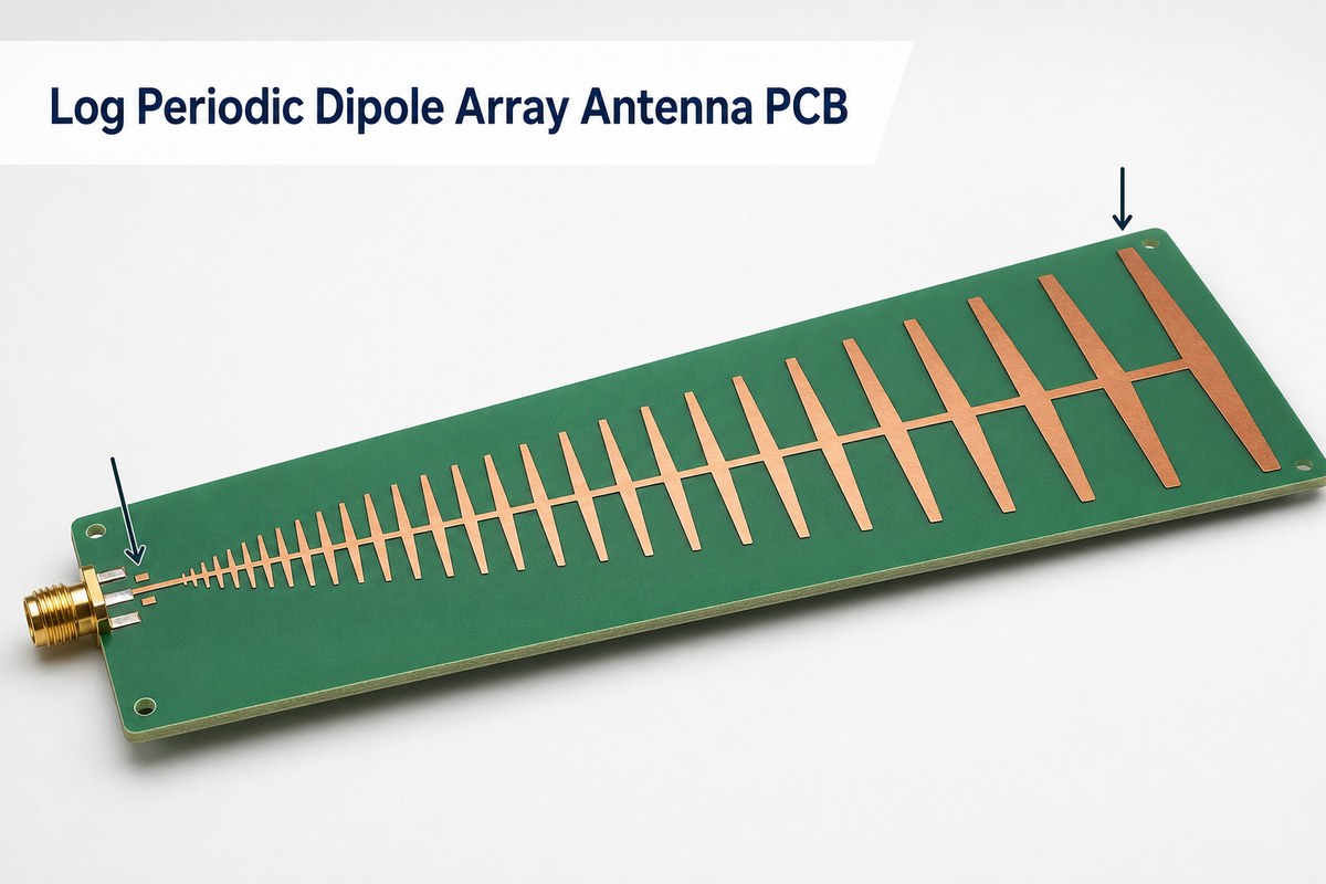
What Is a Log Periodic Dipole Array Antenna PCB?
A printed LPDA is a broadband directional antenna formed by multiple dipoles whose lengths, widths, and positions change by a nearly constant scale ratio. Unlike a conventional PCB carrying an antenna as one small component, the copper pattern, substrate, and feed line are the antenna.
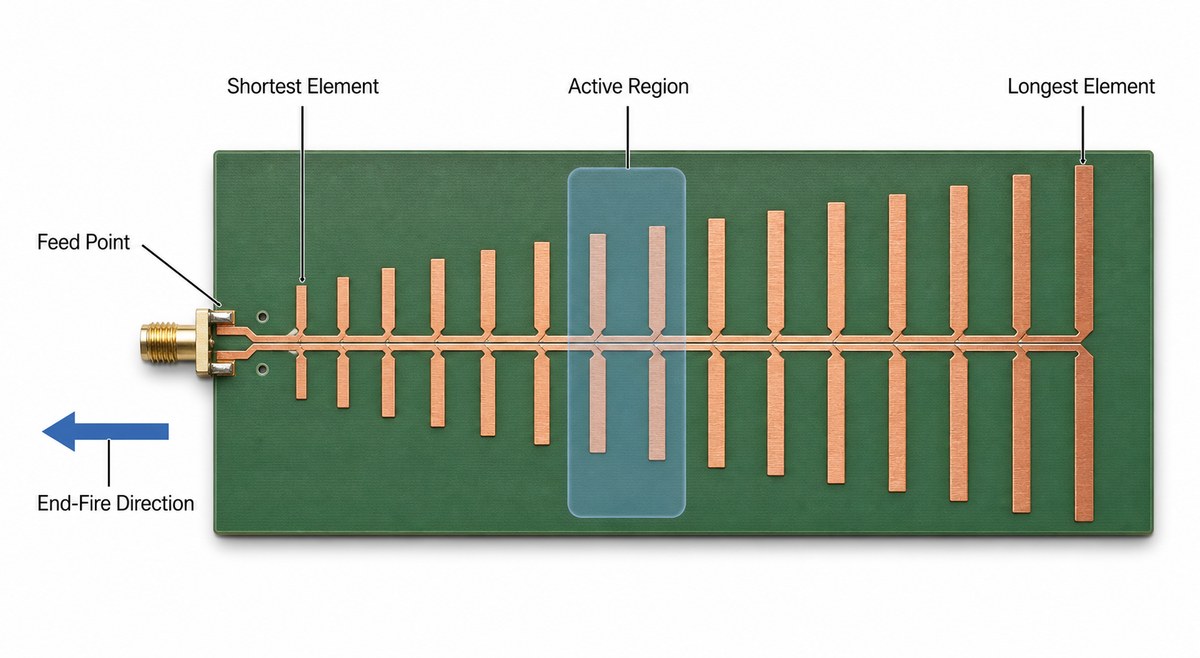
The shortest elements respond near the upper end of the band, while longer elements support progressively lower frequencies. Only a limited group of elements radiates strongly at a given frequency. That group is the active region, and it moves along the array as frequency changes.
How Does a Printed LPDA Cover a Wide Frequency Range?
A printed LPDA covers a wide band by repeating similar dipole cells at progressively scaled sizes. The frequency changes which neighboring elements are close to resonance, so the active region shifts without requiring every element to radiate equally at the same time.
In a conventional arrangement, energy travels along the balanced feed toward the larger elements while adjacent dipoles are connected with alternating polarity. The useful end-fire beam normally points toward the shorter-element end. The exact pattern still needs full-wave simulation and measurement because the substrate, feed, connector, enclosure, cable, and mounting hardware can disturb the ideal behavior.
Log Periodic Dipole Array Design
A useful log periodic dipole array design begins with the target frequency band, desired directional behavior, available board size, feed impedance, and acceptable loss. The scale factor, commonly written as τ, relates adjacent element dimensions. If elements are indexed from larger to smaller, a common definition is τ = Ln+1/Ln, where τ is less than one.
The spacing factor, σ, relates the gap between adjacent elements to element length. These factors influence array length, element count, gain tendency, front-to-back behavior, and impedance variation. They do not determine a finished printed antenna by themselves. The dielectric-loaded geometry and feed still need electromagnetic optimization.
- Set the lower and upper operating frequencies before choosing element count.
- Define whether the quoted bandwidth refers to S11, VSWR, gain, pattern, efficiency, or all of them.
- Reserve margin beyond the nominal band so truncation does not place the active region at the physical edge.
- Model the connector, transition, mounting holes, enclosure, cable route, and nearby metal when they will exist in the product.
Log Periodic Antenna PCB Design
The log periodic antenna pcb design must translate electrical dimensions into a manufacturable copper pattern without changing the current path. Arm length, arm width, element spacing, feed width, feed gap, board thickness, and dielectric properties should remain explicit controlled inputs rather than values left to artwork scaling.
Printed implementations often place alternate arms or feed conductors on opposite sides of the substrate. Others use coplanar or tapered feed arrangements. The correct layer assignment is part of the RF design, not a fabrication convenience. If a layer is mirrored, swapped, or offset, the intended phase relationship can be lost.
| Design Item | Electrical Role | PCB Definition Needed |
| Dipole length | Places each resonant cell within the operating band | Finished copper dimension and etch tolerance |
| Dipole width | Affects impedance, bandwidth, and current distribution | Minimum feature, finished width, and copper thickness |
| Element spacing | Controls coupling and active-region behavior | Finished gap and registration requirement |
| Balanced feed | Sets phase and impedance along the array | Layer pair, width, gap, and dielectric thickness |
| Connector launch | Transfers energy from the cable into the antenna | Connector drawing, pad geometry, edge tolerance, and reference plane |
Which Substrate and Copper Details Matter Most?
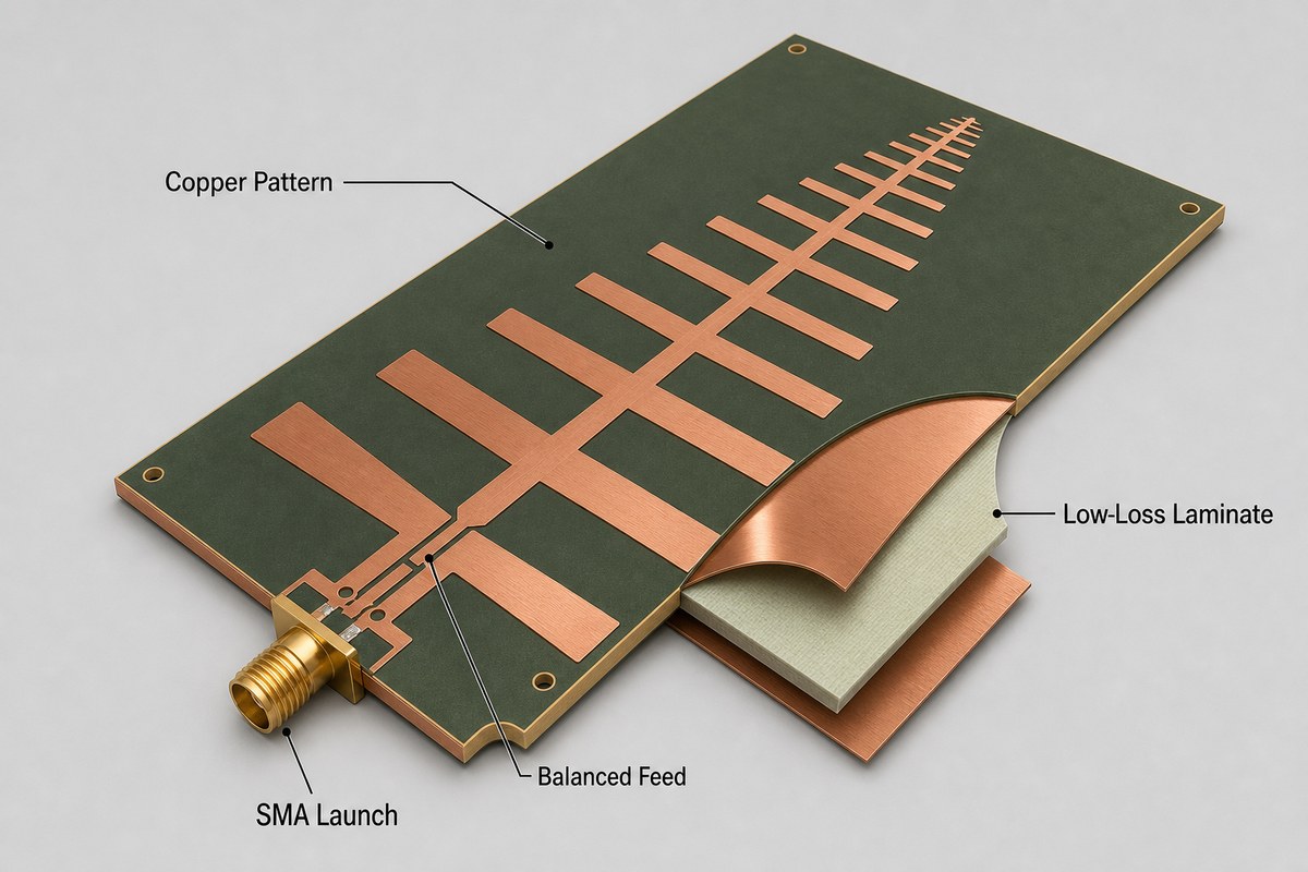
The substrate matters because its dielectric constant changes electrical length, while dielectric loss and copper loss reduce efficiency. Material selection should therefore use the laminate manufacturer’s frequency-dependent data and the values assumed in the electromagnetic model.
FR4 can be a practical prototype or cost-driven option when the frequency range, board size, and loss target are validated. A low-loss RF laminate is usually easier to justify when the band is wide, the upper frequency is high, the feed is long, or unit-to-unit repeatability is tight. Our high-frequency PCB materials guide explains how Dk, Df, copper roughness, and dielectric thickness affect RF boards.
- Specify the exact laminate grade rather than a generic material family.
- State the finished dielectric thickness used in simulation.
- Define base and finished copper thickness where the distinction matters.
- Confirm whether solder mask is kept away from radiating elements and feed structures.
- Review how the selected surface finish changes conductor geometry and loss.
How Should the Feed, Balun, and Connector Transition Be Designed?
The feed must preserve the intended balanced excitation while presenting the required impedance to the external cable or RF circuit. A coaxial connector is unbalanced, while the dipole array is balanced, so the transition should be treated as an RF structure rather than a simple pad connection.
Depending on the topology, the design may use a balanced parallel-strip feed, a microstrip-to-balanced transition, a tapered balun, a coplanar transition, or another simulated structure. The connector body and launch pads should be included in the model. A mathematically correct array can still show poor S11 if the launch adds excess inductance, capacitance, asymmetry, or unwanted common-mode current.
Log Periodic PCB Directional Antenna
A log periodic pcb directional antenna typically produces an end-fire beam toward its shorter elements, with the larger elements behind the active region. This direction should be confirmed in the radiation-pattern result rather than inferred only from the board outline.
LPDA is not automatically the best wideband PCB antenna for every enclosure. A Yagi may be simpler for a narrower band, while a Vivaldi antenna can provide another planar wideband path. The decision depends on band ratio, available length and width, polarization, gain flatness, front-to-back requirement, feed integration, and the surrounding structure.
| Antenna Type | Bandwidth Tendency | Primary PCB Trade-Off |
| Printed LPDA | Wide when the scale, feed, and truncation are optimized | Long tapered array with many tolerance-sensitive cells |
| Printed Yagi | Narrower and more frequency-specific | Simpler element set but less suitable for a large band ratio |
| Vivaldi | Wideband tapered-slot behavior | Needs flare area and a carefully designed feed transition |
Log Periodic PCB Antenna Calculator
A log periodic pcb antenna calculator is useful for generating the first set of element lengths, spacings, and array dimensions. It should not be treated as the final authority for a printed design because many calculators are based on simplified wire-LPDA relationships.
After the initial calculation, transfer the geometry into a full-wave solver with the real substrate, copper thickness, feed, connector, solder mask decision, and mechanical surroundings. Sweep both electrical and manufacturing variables. A design that works only at nominal geometry may drift after ordinary etching, material, or registration variation.
- Document the calculator equations and the direction in which elements are indexed.
- Keep the original target band separate from the wider simulation sweep.
- Run sensitivity studies for Dk, dielectric thickness, copper width, and feed gap.
- Export dimensioned fabrication data; do not ask the factory to recreate RF geometry from a screenshot.
Which Fabrication Tolerances Can Shift RF Performance?
The most sensitive fabrication variables are the ones that change resonant length, coupling, or feed impedance. On a wideband array, a small error repeated across many elements can alter gain flatness or create a local mismatch even when the board passes continuity testing.
- Etch variation: changes arm width, arm length, feed width, and the gaps between conductors.
- Dielectric variation: changes electrical length and feed impedance.
- Layer registration: matters when alternate arms or balanced conductors occupy opposite sides.
- Board outline and connector position: affect the launch and the mechanical reference.
- Solder mask and surface finish: can add dielectric loading or change the conductor surface.
- Handling and mounting: can bend a long thin board or bring metal hardware into the near field.
Controlled impedance is relevant to the feed, but it does not certify the antenna pattern. Review the feed geometry with the same discipline used for a radio frequency PCB, then keep the radiating elements under their own dimensional controls.
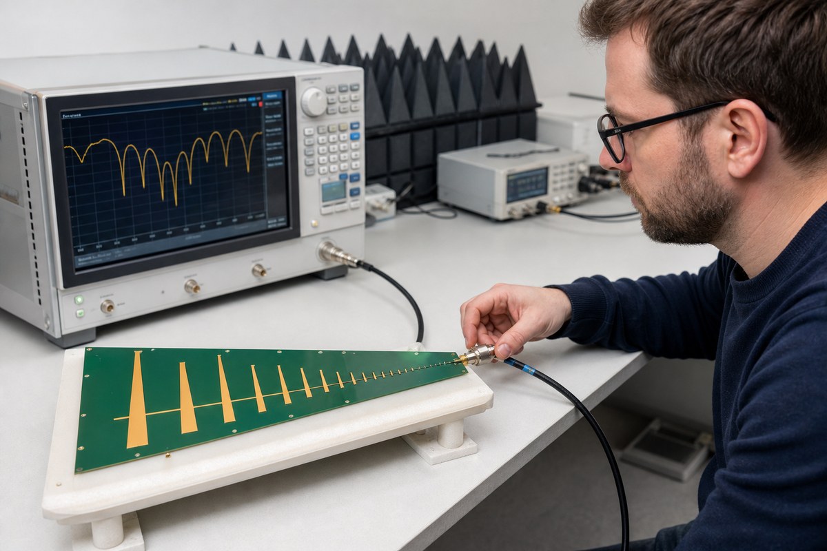
How Should a Fabricated LPDA PCB Be Tested?
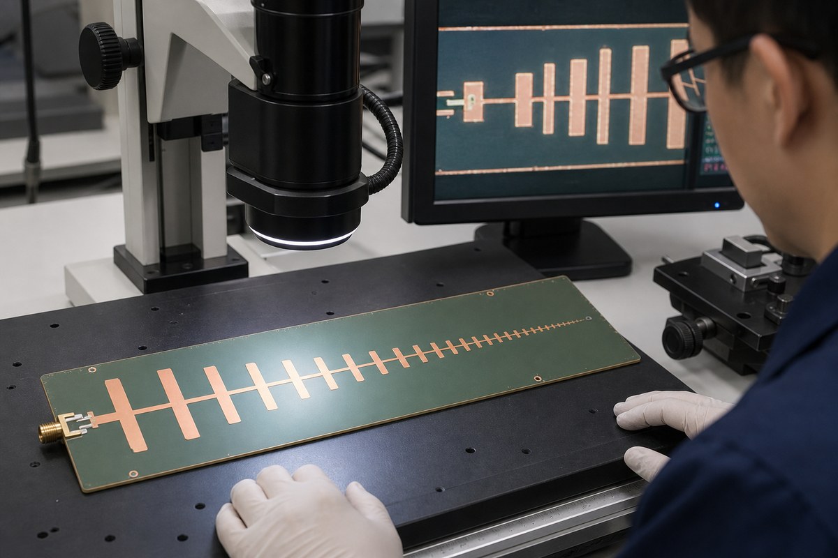
A fabricated LPDA should be checked in stages: dimensional inspection first, port matching next, and radiation performance last. These tests answer different questions and should not be collapsed into a single pass/fail statement.
- Inspect the bare PCB: verify critical lengths, widths, gaps, registration, outline, connector position, and visible defects.
- Prepare the RF fixture: use the intended connector and mounting condition, then calibrate the VNA to a defined reference plane.
- Measure S11 or return loss: sweep beyond the target band to see edge behavior and unexpected resonances.
- Measure radiation performance: verify pattern direction, gain, beamwidth, front-to-back behavior, polarization, and efficiency when those are acceptance requirements.
- Compare samples: separate design error from fabrication variation by reviewing geometry and material records with the RF results.
A bare-board electrical test can find opens and shorts, but it cannot prove antenna gain or radiation pattern. Likewise, a good S11 trace does not guarantee that accepted power is radiated in the intended direction. The test plan must match the product’s actual RF acceptance criteria.
What Data Should Be Included in an LPDA PCB Fabrication Package?
The fabrication package should define every board variable that the RF model assumes. Gerber or ODB++ data alone may show the artwork, but it may not explain the material values, controlled dimensions, connector reference, or acceptance method.
- Gerber or ODB++ data, drill files, and a dimensioned drawing.
- Exact laminate grade, finished dielectric thickness, and copper construction.
- Critical finished dimensions and tolerances for elements, feed, and gaps.
- Layer order, polarity, and registration requirements for balanced structures.
- Surface finish and solder mask clearance instructions.
- Connector part number, launch drawing, and board-edge requirements.
- Target band, reference impedance, and available simulation or acceptance data.
- Prototype quantity, production quantity, panel constraints, and assembly scope.
If the design uses a specific low-loss laminate, review its availability and processing route before freezing the stackup. The Rogers RO3010 material guide shows why material grade and dielectric data must be explicit in compact RF structures.
FAQ About Log Periodic Dipole Array Antenna PCBs
Is every printed LPDA automatically wideband?
No. The log-periodic geometry supports wideband behavior, but the useful band also depends on truncation, the feed transition, substrate, connector, material loss, nearby structures, and the acceptance metric.
Can FR4 be used for a printed LPDA?
Yes, if simulation and measurement show that its loss and dielectric variation are acceptable for the target band, board size, gain, and repeatability. A low-loss laminate may be safer when those margins are tight.
Does the longest dipole set the lower frequency limit?
It strongly influences the low-frequency edge, but the final limit also depends on dielectric loading, element width, spacing, feed behavior, and truncation margin. Do not size it from free-space half wavelength alone.
Which direction does an LPDA antenna radiate?
A conventional LPDA normally points toward its shorter elements. Confirm the actual main-beam direction in the simulated and measured pattern because feed and mechanical details can change the result.
Can PCB inspection replace antenna testing?
No. Dimensional inspection and electrical testing verify the board, while VNA and radiation measurements verify RF behavior. Both are needed when the antenna has formal performance requirements.
How Can EBest Circuit Support Your LPDA Antenna PCB?
At EBest Circuit, we support RF and high-frequency PCB projects with material and stackup review, controlled-impedance fabrication, prototypes, production orders, PCB assembly, and inspection. For an LPDA project, we can review the manufacturing data and identify board-level details that need clearer tolerances before production; final antenna performance remains tied to your validated RF design and test plan.
Send your Gerber or ODB++ files, stackup, laminate grade, target frequency band, connector drawing, critical tolerances, quantity, and available RF acceptance data to sales@bestpcbs.com. We will review the Log Periodic Dipole Array Antenna PCB fabrication requirements and prepare the appropriate PCB or PCBA quotation.
You may also like





Tags: log periodic antenna pcb design, Log Periodic Dipole Array Antenna PCB, log periodic dipole array design, log periodic pcb antenna calculator, log periodic pcb directional antenna