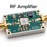
An rf amp circuit is used to increase the strength of a radio frequency signal before it reaches an antenna, receiver stage, RF module, coaxial cable, or test system. For engineers and buyers, the practical question is not only how the circuit works, but whether the RF amplifier board can be manufactured, assembled, inspected, and tested reliably.
That is where PCB and PCBA review becomes important. An RF amp circuit may involve controlled impedance, SMA connectors, RF materials, grounding, shielding, copper thickness, thermal control, component placement, soldering, and RF testing. EBest Circuit (Best Technology) supports RF-related PCB fabrication, component sourcing, SMT assembly, through-hole assembly, inspection, and small-batch PCBA projects. If your RF amplifier project is ready for manufacturing review, please send your Gerber files, stackup, BOM, RF notes, connector drawing, and test requirements to sales@bestpcbs.com.
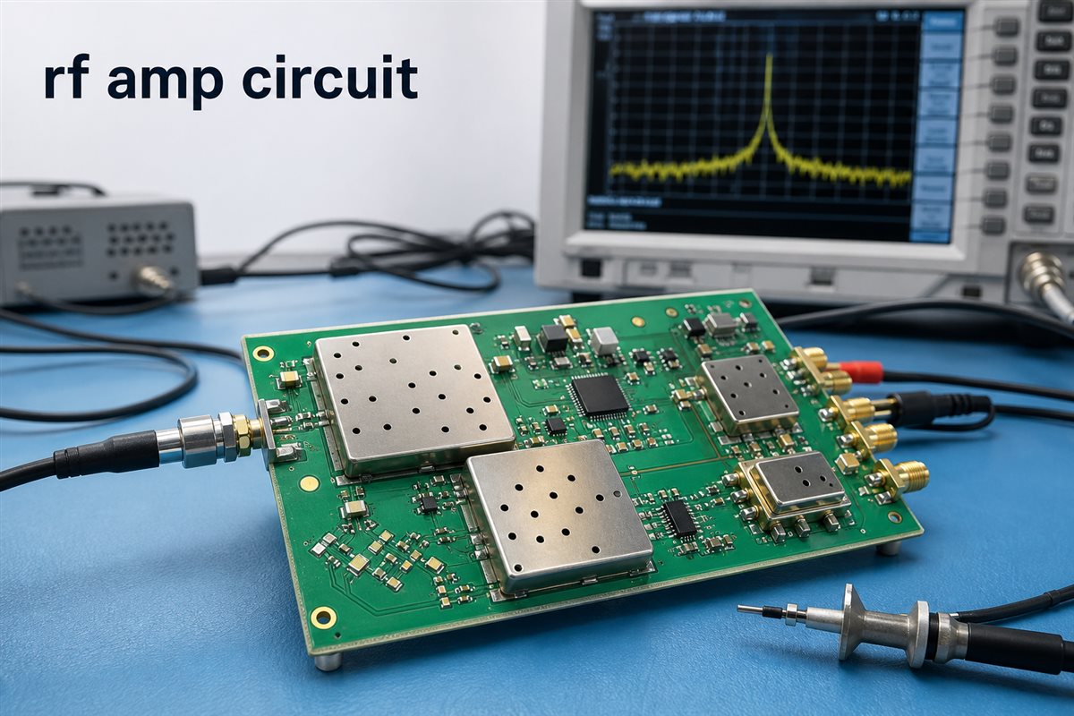
What Is an RF Amp Circuit?
An RF amp circuit is a radio frequency amplifier circuit that increases RF signal power, voltage, or current within a specified frequency range.
It may be used in:
- wireless communication modules
- RF test equipment
- antenna systems
- receiver front ends
- transmitter output stages
- IoT and telemetry products
- industrial RF modules
- medical or sensing equipment
- satellite or base station related products
The exact circuit function depends on the customer’s RF design. Some RF amplifiers focus on low noise. Some focus on output power. Some need wide bandwidth. Some need high linearity. Some must work with a 50 ohm RF path and SMA or coaxial connectors.
For PCB manufacturing, the most important point is not to redesign the amplifier. The customer’s RF design team should define the frequency, gain, active components, matching network, and performance target. The PCB manufacturer’s role is to help turn approved circuit files into a stable PCB or PCBA build.
RF Amp Circuit vs RF Amplifier Circuit
In many searches, rf amp circuit and rf amplifier circuit mean almost the same thing. “Amp” is simply a shorter way to say “amplifier.”
However, the wording can reveal different user expectations:
| Search Term | Common Search Intent |
| rf amp circuit | Short search for circuit explanation, example, or board project |
| rf amplifier circuit | More formal circuit explanation |
| radio frequency amplifier circuit | Educational explanation or technical reference |
| rf power amplifier circuit | Higher output power or transmitter-related circuit |
| rf amplifier module | Product/module level search |
| amplifier circuit PCB | PCB manufacturing or assembly angle |
For this article, the focus is not only the circuit idea. The focus is what happens when an RF amplifier circuit becomes a manufacturable PCB and PCBA project.
If the board is poorly laid out or poorly assembled, even a correct schematic may perform badly. Problems such as impedance discontinuity, poor grounding, long RF traces, wrong connector footprint, weak solder joints, heat buildup, or shield contact issues can affect the final result.
RF Power Amplifier Circuit vs Low Noise Amplifier Circuit
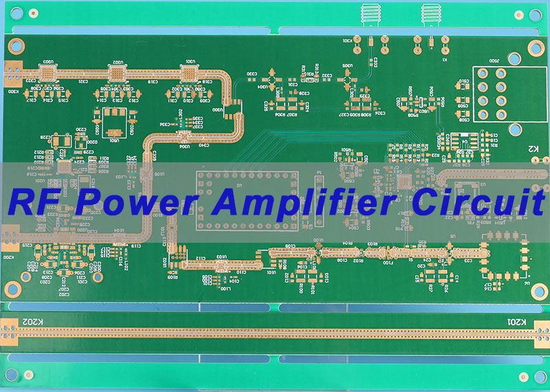
RF amplifier circuits are not all the same. Two common categories are RF power amplifier circuits and low noise amplifier circuits.
| Circuit Type | Main Goal | PCB/PCBA Concern |
| RF power amplifier circuit | Increase output power | Heat, copper, grounding, current path |
| Low noise amplifier circuit | Preserve weak signal quality | Noise, shielding, short RF path |
| Broadband RF amplifier | Work across wide frequency range | Stable impedance and layout symmetry |
| RF driver amplifier | Drive the next RF stage | Matching and thermal stability |
| RF module amplifier | Integrated product function | Connector, enclosure, testing |
For a power amplifier, copper thickness, heat spreading, via placement, component derating, and solder joint strength may become important. For a low noise amplifier, the layout is usually more sensitive to grounding, shielding, leakage paths, component placement, and noise coupling.
EBest Circuit does not decide the amplifier topology for the customer. That belongs to the RF design side. Our value is to review whether the PCB files, stackup, material, assembly notes, and test requirements match the manufacturing path.
Radio Frequency Amplifier Circuit Diagram and PCB File Review
A radio frequency amplifier circuit diagram is only one part of the production package. Before a board can move into fabrication and assembly, the manufacturer needs enough files to understand both the electrical and mechanical requirements.
Useful production files include:
- Gerber or ODB++ files
- PCB stackup drawing
- BOM with approved part numbers
- CPL / pick-and-place file
- Assembly drawing
- Schematic or RF notes when allowed
- Connector datasheets
- Controlled impedance requirements
- SMA or coaxial connector drawing
- Shielding or enclosure notes
- Testing requirements
- Packing and labeling requirements
For RF projects, missing information can create real production risk. For example, a connector may appear correct in the BOM but require a specific board thickness, edge clearance, solder pad geometry, or mounting style. A controlled impedance trace may be drawn correctly in layout software but still need stackup confirmation before fabrication.
Before production, EBest Circuit can review the manufacturing files and raise EQ questions if something needs confirmation. This is especially useful when the project includes RF connectors, impedance control, high-frequency material, shielding cans, or mixed SMT and through-hole assembly.
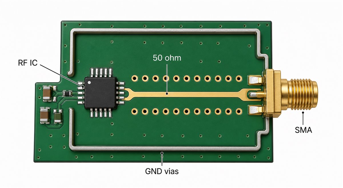
50 Ohm Impedance in RF Amp Circuit PCB Manufacturing
Many RF amp circuit boards use a 50 ohm signal path. This is common for RF test equipment, coaxial cables, SMA connectors, antennas, RF modules, and many communication systems.
A 50 ohm path is affected by trace width, copper thickness, dielectric thickness, material dielectric constant, solder mask condition, reference plane distance, connector transition, via structure, and manufacturing tolerance.
The 50 ohm requirement should be confirmed before fabrication, not only checked after the board is made. If impedance control is required, the stackup, trace width, dielectric thickness, copper thickness, and test coupon should be reviewed together.
For RF PCBs, EBest Circuit can support controlled impedance review and provide impedance test reports when required by the customer. For related RF material and manufacturing options, customers can also review our RF PCB capability page.
SMA Connectors, Grounding, and Shielding in RF Amp Circuit Boards
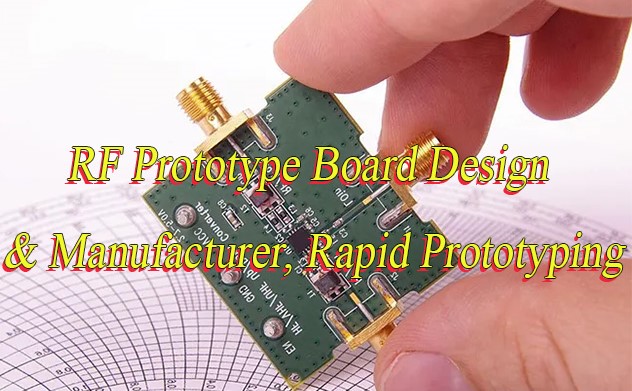
SMA connectors are common in RF amp circuit boards because they provide a practical interface between the PCB and coaxial cable, antenna, RF instrument, or external module.
SMA connector reliability depends on more than the part number.
Key manufacturing details include:
- PCB thickness at the connector area
- edge-launch or through-hole connector type
- center pin pad geometry
- ground terminal contact
- solder mask opening
- mounting hole or flange requirement
- connector height and mechanical clearance
- coaxial cable direction
- soldering method
- final inspection access
Grounding and shielding are equally important. RF amplifier boards may use ground vias, via fences, shielding cans, connector shell grounding, enclosure contact, or separated RF and power areas. If the board uses a shielding can, the solder pads must allow stable attachment. If the project uses board-level shielding, the PCBA process should keep shield placement, soldering, and inspection clear.
A related EMI shield PCB article may be useful when the RF amplifier board also has shielding structures or enclosure-level EMI control.
RF Amp Circuit PCB Materials and Stackup Choices
The material choice for an RF amp circuit board depends on frequency, loss requirement, board thickness, cost target, thermal need, and the customer’s approved RF design.
Common options may include:
- standard FR4 for lower-frequency or cost-sensitive RF products
- high-Tg FR4 for better thermal and process margin
- Rogers or other RF laminate for lower loss or tighter RF performance
- hybrid stackup when RF and digital/power sections share one board
- metal core or thermal structure when heat is a major concern
Not every RF amplifier board needs expensive RF laminate. Some lower-frequency or less sensitive projects can be manufactured with carefully controlled FR4. However, higher-frequency, high-power, low-noise, or insertion-loss-sensitive projects may require better material control.
For manufacturing review, the stackup should match the RF path, power path, grounding strategy, assembly method, and mechanical requirement. A stackup that looks acceptable electrically but is difficult to laminate, drill, plate, or assemble may create production risk.
Thermal Control for RF Power Amplifier Circuit Boards
RF power amplifier circuits can generate heat. If the heat is not controlled, performance and reliability may suffer.
Thermal review may involve:
- copper thickness
- large copper areas
- thermal vias
- component pad design
- heat spreading path
- board thickness
- solder joint reliability
- component derating
- shield or enclosure heat path
- test condition and operating duty cycle
For higher-power RF boards, the heat path should be discussed before production. The PCB manufacturer can review copper thickness, via process, material selection, solderability, and assembly feasibility, but the customer should define the power level, thermal simulation target, enclosure condition, and operating environment.
If the project is related to a higher-power amplifier, our previous article on high power RF amplifier circuit can be used as a supporting reference.
SMT Assembly and Testing for RF Amp Circuit PCBA
RF amp circuit PCBA projects often include small RF components, SMA connectors, shield cans, regulators, matching components, filters, inductors, capacitors, and sometimes through-hole or mechanical parts.
Small quantity does not mean low process risk.
Assembly risks may include:
- wrong RF component value
- component rotation
- poor solder wetting
- tombstoning of small passives
- SMA solder joint weakness
- shield can solder gap
- connector tilt
- flux residue near RF areas
- thermal pad voiding
- inspection blind spots
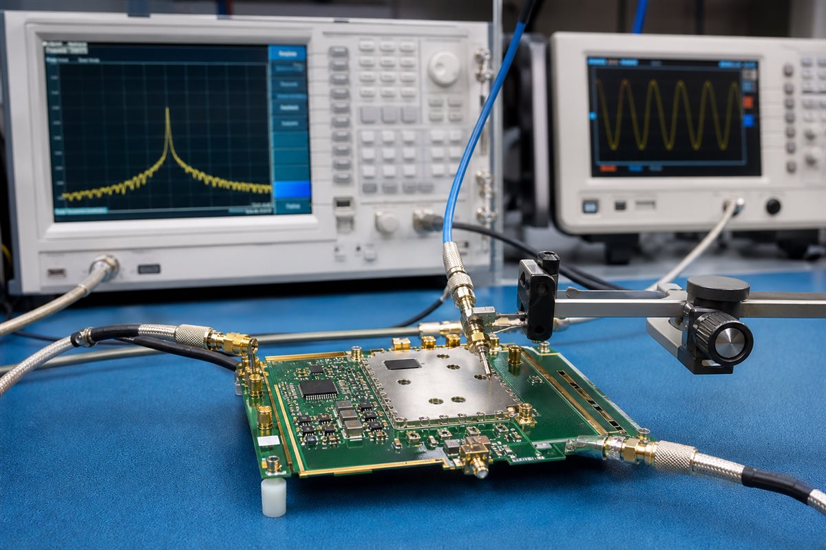
Testing also needs planning. Some projects only need visual inspection and electrical continuity. Others may require RF performance testing, functional testing, programming, or fixture-based verification. When RF test requirements are defined by the customer, EBest Circuit can coordinate the manufacturing and assembly side so the boards are prepared for the required test method.
For PCBA projects, the most useful test notes are practical: test points, connector access, pass/fail criteria, fixture needs, labeling method, and packing requirements.
RF Amp Circuit Manufacturing Case Study
A U.S. customer needed a small batch of RF amplifier PCB assemblies for a wireless test module used during engineering validation. The board was not a simple FR4 prototype. It needed stable RF transmission, connector reliability, clean assembly, and test-ready delivery.
Project requirements:
- Customer region: USA
- Application: Wireless RF test module
- Quantity: 20 pcs pilot build
- PCB type: 4-layer RF amplifier PCB
- Material: High-Tg FR4 with RF path review
- Finished thickness: 1.6mm +/-10%
- Copper thickness: 1oz finished copper
- Surface finish: ENIG
- Connector: SMA interface for RF input/output
- Impedance: 50 ohm RF trace control
- Assembly: SMT + connector assembly
- Testing: Visual inspection, electrical test, and customer-defined RF test preparation
- Delivery target: Prototype-to-pilot build schedule
Manufacturing challenges:
- The SMA connector footprint and board thickness had to match the connector drawing.
- The 50 ohm RF trace needed stackup and trace geometry review before fabrication.
- Ground via placement and shield-related pads had to remain clear for assembly.
- Small RF passives required correct orientation and stable SMT control.
- The customer needed boards packed safely for lab validation after assembly.
EBest Circuit solution:
- Reviewed Gerber, stackup, BOM, CPL, connector drawing, and RF notes together.
- Confirmed the impedance structure before production.
- Checked SMA pad geometry, grounding area, solder mask opening, and connector clearance.
- Prepared PCB fabrication and SMT assembly under one workflow.
- Inspected connector solder joints, RF component placement, board cleanliness, and packing method.
- Kept production notes visible from file review to final shipment.
Result:
The customer received 20 RF amplifier PCB assemblies ready for engineering validation. The value was not only making the PCB. The value was keeping RF path, connector mounting, impedance control, SMT assembly, inspection, and packing details connected before the boards reached the customer’s test bench.
This is the type of project where one unclear connector note or one missed impedance requirement can delay the whole validation schedule. A controlled manufacturing review helps reduce that risk before the pilot build starts.
Why Choose EBest Circuit for RF Amp Circuit PCB Projects?
EBest Circuit is suitable for RF amp circuit PCB and PCBA projects when the customer needs more than bare board fabrication.
What EBest Circuit can support:
- RF PCB fabrication
- FR4, high-Tg FR4, RF laminate, and hybrid material review
- Controlled impedance review
- SMA and RF connector assembly support
- SMT assembly and through-hole assembly
- Component sourcing based on approved BOM
- DFM and assembly file review
- Electrical testing and inspection
- Small-batch and pilot production
- Packing and delivery coordination
EBest Circuit has worked in PCB and PCBA manufacturing since 2006. The company supports prototype, small-batch, and production projects for customers in more than 40 countries and regions. Quality support includes ISO9001, ISO13485, IATF16949, AS9100D, RoHS, REACH, and UL-related documentation.
For RF amp circuit projects, stable engineering communication matters. The board may involve RF traces, connectors, controlled impedance, shielding, thermal concerns, and assembly details at the same time. EBest Circuit’s engineering and production teams can help keep those details visible before fabrication and assembly begin.
FAQs About RF Amp Circuit
1. What is an RF amp circuit?
An RF amp circuit is a radio frequency amplifier circuit used to increase RF signal strength within a defined frequency range. It may be used in wireless modules, antenna systems, RF test equipment, transmitters, receivers, and communication products.
2. Is an RF amp circuit the same as an RF amplifier circuit?
Yes, in most searches they mean the same thing. “RF amp circuit”is a shorter phrase, while “RF amplifier circuit”is the more formal term.
3. Does an RF amp circuit PCB always need 50 ohm impedance?
Not always, but many RF amplifier boards use 50 ohm paths because SMA connectors, coaxial cables, antennas, and RF instruments commonly use 50 ohm systems. The exact requirement should come from the customer’s RF design.
4. Can EBest Circuit design the RF amplifier circuit?
EBest Circuit does not replace the customer’s RF design team. The active device, topology, gain target, matching network, and RF performance target should come from the customer. EBest Circuit can review PCB manufacturability, stackup, impedance, connector mounting, assembly, and testing requirements.
5. What files should I send for RF amp circuit PCB manufacturing?
Useful files include Gerber or ODB++, stackup drawing, BOM, CPL file, assembly drawing, connector datasheets, impedance notes, RF test requirements, and packing instructions.
All in all, an rf amp circuit project is not only about the amplifier schematic. It is about making sure the RF path, PCB material, impedance, connector, grounding, shielding, assembly, inspection, and testing requirements can move through production without avoidable confusion. If your project is ready for PCB or PCBA review, please send your files and questions to sales@bestpcbs.com.
You may also like




Tags: rf amp circuit, rf amplifier circuit, RF Power Amplifier Circuit