A heavy copper PCB manufacturer should help you control copper weight, trace width, spacing, via plating, heat rise, DFM risk, PCBA fit and quote scope before fabrication starts. Heavy copper boards are usually used when a standard PCB cannot safely carry the required current or dissipate heat from power devices, relays, converters, motor drives, LED drivers or industrial control circuits.
EBest Circuit supports heavy copper PCB buyers with heavy copper PCB manufacturing, engineering review, DFM feedback, high-current design discussion, optional PCBA support and RFQ planning. Send the copper weight, current path, stackup, drawings, Gerber or ODB++, quantity and test requirements early so the build can be reviewed as a high-current board, not a normal FR4 order.
What Should a Heavy Copper PCB Manufacturer Control?
A heavy copper PCB manufacturer should control the full high-current structure, not only quote a thicker copper layer. Copper weight affects trace width, etching, spacing, solder mask, via plating, thermal rise, board thickness, panel yield, assembly clearance and cost.
For buyers, the practical question is whether the supplier can explain what is standard, what is special, and what must be reviewed from the files. If a design uses 3 oz, 4 oz, 5 oz or higher copper, a normal PCB design rule cannot be copied blindly into the RFQ.
Is your high-current PCB quote unclear because copper weight changes the whole build?
Heavy copper PCB projects often slow down before approval when the buying package misses key manufacturing details:
- The design asks for thick copper, but trace width, spacing and solder mask bridge were not adjusted for the selected copper weight.
- The current path runs through vias, connectors or terminals, but plating thickness and thermal rise have not been reviewed together.
- The quote compares only board price, while DFM feedback, PCBA clearance, testing and production repeatability are not included.
- The buyer is unsure whether the requested copper weight is a normal process, special process or file-dependent review item.
- Assembly requirements arrive after fabrication planning, creating late changes around pads, terminals, heat sinks and test fixtures.
Where High-Current PCB Projects Usually Lose Time
High-current PCB projects usually lose time when copper weight is treated as an isolated specification. Thick copper changes how traces are etched, how close features can sit, how vias carry current, how solder mask covers edges, and how the assembled board handles heat.
The fastest route is to review the copper path before the purchase order is placed. A useful RFQ should tell the manufacturer where current enters, where it returns, what temperature rise is acceptable, which layers carry current and whether the board will need high-current testing or functional inspection after assembly.
EBest Circuit helps buyers turn thick-copper uncertainty into a manufacturable quote package:
- We review copper weight, layer stackup, trace width, spacing, via structure, board thickness, finish and drawings together.
- We separate normal capability from special review items so buyers do not rely on unsupported assumptions.
- We connect fabrication review with PCBA planning when terminals, relays, power packages, heat sinks or test fixtures affect the final board.
- We help compare quote scope, not only unit price, so prototype and production decisions are easier to defend.
How EBest Circuit Reviews Heavy Copper PCB Builds
EBest Circuit reviews heavy copper PCB builds by checking copper weight, geometry, current path and assembly needs before fabrication. The review starts with the board files and drawing, then checks whether the copper specification matches trace/space, holes, via plating, solder mask, finish, board thickness, panelization and inspection expectations.
This approach matters because a high-current design can fail even when the copper weight looks strong on paper. Bottlenecks may appear at vias, terminal pads, neck-down traces, layer transitions, thermal hot spots or assembly joints. These are project details, not generic catalog promises.
Copper Weight: Normal Range vs Special Review
Heavy copper PCB capability must be stated with conditions because copper weight changes the manufacturing route. EBest Circuit’s verified FR4 capability source lists inner copper from 0.5 oz to 5 oz as a normal range, and 5 oz to 20 oz as a special capability. It lists outer copper from 1 oz to 5 oz as a normal range, and 5 oz to 20 oz as a special capability.
| Layer Area | Verified Normal Range | Special Review Range | Buyer Action |
|---|---|---|---|
| FR4 inner layer copper | 0.5 oz to 5 oz | 5 oz to 20 oz | Send stackup and current path for review |
| FR4 outer layer copper | 1 oz to 5 oz | 5 oz to 20 oz | Confirm spacing, pads, finish and assembly clearance |
Trace Width, Spacing and Copper Balance
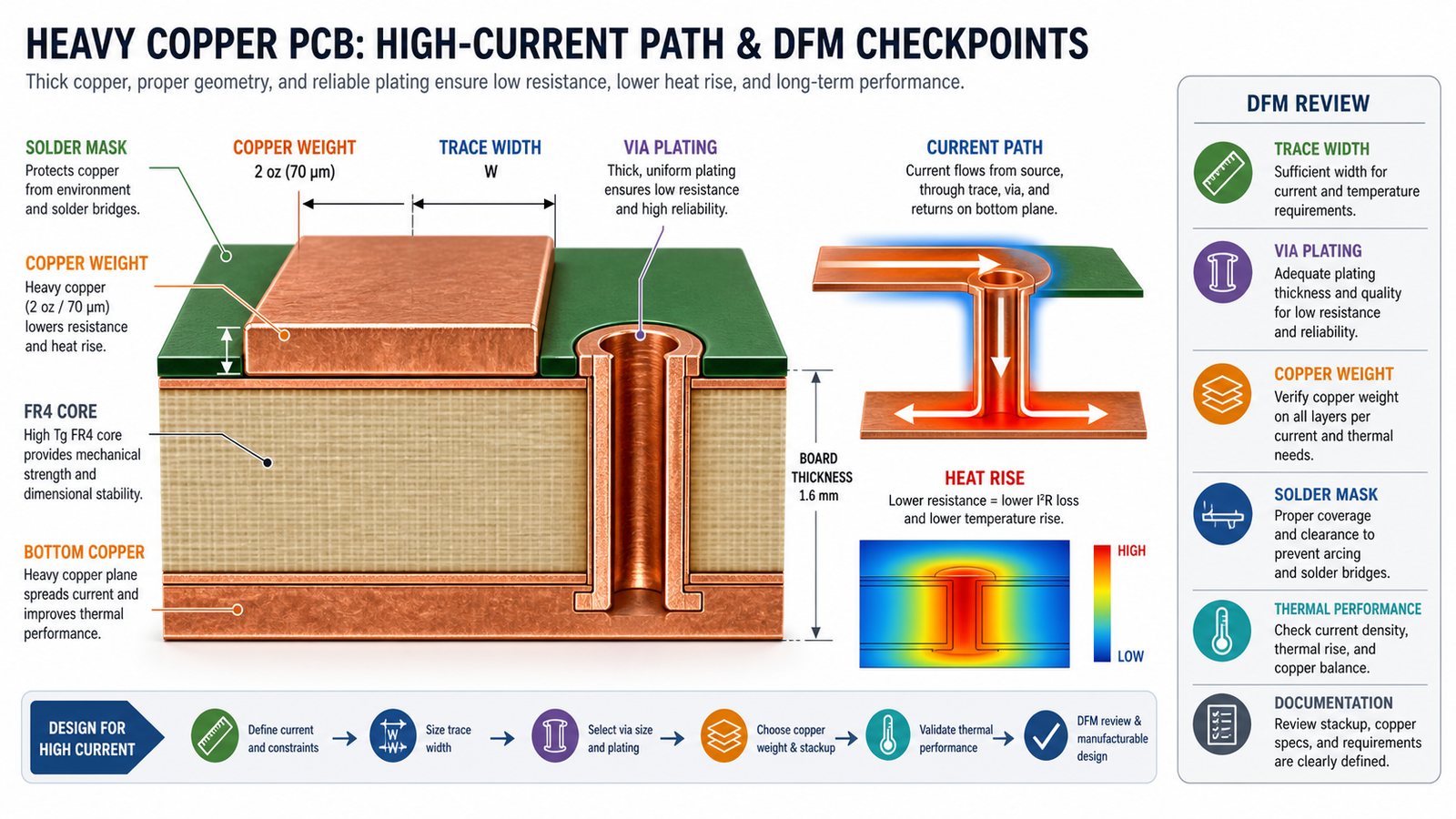
Trace width and spacing must increase as copper weight increases because thick copper cannot use the same geometry as thin copper. Verified examples show why file review is needed: 2/2 oz uses 6/6 mil as a normal example, 3/3 oz uses 10/12 mil, 4/4 oz uses 12/16 mil, and 5/5 oz uses 16/20 mil. Special routes can be tighter in some cases, but they require review.
For a buyer, this means the PCB layout should not be released to fabrication only because the current calculator says a trace is wide enough. The manufacturing rule, solder mask clearance, copper balance and PCBA clearance must also match the selected copper weight.
Via Plating, Current Path and Thermal Rise
Via plating and current path review are essential for heavy copper PCB reliability. A thick top trace does not help if the current necks down through weak vias, narrow internal connections, under-sized pads or poorly balanced copper areas.
Ask the manufacturer to review where current enters, how it transfers between layers, where heat may concentrate, and whether terminals, screws, connectors or busbar-style copper areas need special fabrication or assembly planning.
Heavy Copper PCB Manufacturing Process
The heavy copper PCB manufacturing process needs closer control of imaging, etching, plating, solder mask and inspection than a standard PCB build. The process normally starts with file intake and DFM review, then material preparation, imaging, etching, drilling, plating, solder mask, surface finish, routing, electrical test and inspection.
As copper gets thicker, the process window becomes narrower. Etching can affect sidewalls, solder mask may need more clearance, and plating must support the current path. That is why the RFQ should include drawings and copper details instead of only Gerber files.
DFM Checks Before Heavy Copper Fabrication
DFM review before heavy copper fabrication should check every place where copper thickness changes manufacturability. Review trace width, spacing, copper balance, annular ring, via count, plating, solder mask bridge, surface finish, thermal relief, board thickness, outline and assembly clearance.
EBest Circuit can also connect this review with the heavy copper PCB design guide and project-specific feedback so the buyer understands which adjustments reduce risk before the board is released.
PCBA Support for Power Electronics Boards
PCBA support should be planned early when a heavy copper PCB carries relays, terminals, MOSFETs, transformers, connectors or other power components. These parts can affect pad design, solder volume, thermal relief, inspection access and test strategy.
If your project needs assembly, send BOM, CPL, assembly drawings, polarity notes and test requirements with the PCB RFQ. For prototype work, EBest Circuit can also coordinate prototype PCB assembly so fabrication and assembly risks are reviewed together.
Heavy Copper PCB Cost Drivers
Heavy copper PCB cost depends on copper weight, board size, layer count, spacing, drilling, plating, finish, inspection and assembly scope. A low quote may become expensive if it leaves out special copper review, PCBA clearance or testing.
| Cost Driver | Why It Matters | RFQ Control Point |
|---|---|---|
| Copper weight | Controls etching, spacing, plating and material cost | State finished copper per layer |
| Geometry | Thick copper needs wider spacing and better copper balance | Send design rules and drawings |
| PCBA scope | Power components can change soldering and inspection needs | Send BOM, CPL and assembly notes |
| Testing | High-current boards may need more than bare electrical test | Define functional or current-load test expectations |
RFQ Checklist for Heavy Copper PCB Manufacturing
A heavy copper PCB RFQ should show the manufacturer how current, heat and copper geometry work together. Include these items when possible:
- Gerber or ODB++ files.
- Stackup and finished copper weight per layer.
- Fabrication drawing, board thickness and surface finish.
- Current path notes, expected current and acceptable temperature rise if known.
- Drill, via, plating and terminal requirements.
- BOM, CPL, assembly drawing and test requirements for PCBA projects.
- Prototype, low-volume and production quantities.
Why Add EBest Circuit to Your Quote List?
EBest Circuit is worth adding to your heavy copper PCB quote list because high-current boards need engineering review, not only a quick price. We support industrial, power electronics, LED driver, control system, communication and small-to-medium batch projects where current capacity, thermal behavior, PCBA coordination and production planning matter.
Compared with a quote-only path, EBest Circuit helps buyers identify copper, geometry, plating, assembly and test questions before they become order delays. You can also review our high current PCB manufacturer article and heavy copper PCB for power electronics guide for related buying context.
FAQ About Heavy Copper PCB Manufacturers
What is a heavy copper PCB manufacturer?
A heavy copper PCB manufacturer fabricates printed circuit boards with thicker copper layers for high-current or thermal applications. The manufacturer should review copper weight, spacing, via plating, thermal rise, PCBA needs and testing before quoting.
What copper weight counts as heavy copper?
Many buyers use the term heavy copper for boards above standard copper weights, often around 3 oz and higher. The exact manufacturing route depends on layer structure, geometry, finished copper and project requirements.
Can EBest Circuit support 5 oz to 20 oz copper?
EBest Circuit’s verified FR4 capability source lists 5 oz to 20 oz as special capability for inner and outer copper. This should be reviewed from the actual files, stackup and geometry before quotation.
Why does heavy copper need wider spacing?
Thicker copper changes etching and solder mask behavior. Wider spacing helps maintain manufacturability, insulation clearance and production consistency. The required spacing depends on copper weight and layout.
Final Recommendation
Choose a heavy copper PCB manufacturer that checks copper weight, geometry, current path and PCBA scope before quoting. Thick copper alone does not guarantee a reliable high-current board; the full manufacturing and assembly plan must match the electrical load.
If you are preparing a heavy copper PCB or high-current PCBA project, send Gerber or ODB++, stackup, copper weight per layer, fabrication drawing, BOM, CPL, quantity, current path notes, surface finish, test requirements and target schedule to sales@bestpcbs.com. EBest Circuit will review the files and help you build a clearer heavy copper PCB manufacturing quotation path.