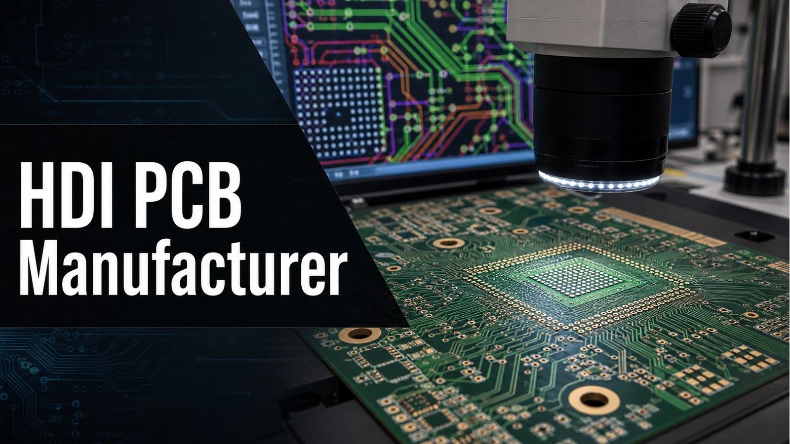
An HDI PCB manufacturer should help you control stackup, microvia structure, blind and buried vias, BGA escape, fine traces, DFM risk, inspection and quote scope before fabrication starts. HDI boards are not simply smaller PCBs; they use high-density interconnect structures that can make a compact product possible, but they also increase manufacturing sensitivity.
EBest Circuit supports HDI PCB buyers with fabrication review, HDI PCB manufacturing support, DFM feedback, material discussion, optional PCBA coordination and RFQ planning. If your board uses microvias, tight BGA routing, blind/buried vias or compact multilayer stackups, send the files early so the build can be reviewed before quotation.
What Should an HDI PCB Manufacturer Help You Control?
An HDI PCB manufacturer should help control the high-density parts of the design that standard PCB quoting often misses. The key questions are not only layer count and price. Buyers need to know whether the stackup, via structure, laser drilling, annular ring, trace/space, copper, solder mask, surface finish and inspection plan match the actual product risk.
For engineering teams, HDI is usually chosen to solve BGA fanout, smaller product size, higher routing density or shorter signal paths. For purchasing teams, the supplier decision should also cover manufacturability, quote clarity, revision risk and whether the same manufacturer can support prototype, low-volume and repeat builds.
Is your HDI PCB project hard to quote because the risk is hidden inside the stackup?
Many HDI PCB projects slow down before approval because the buying package does not expose the manufacturing risk clearly enough:
- The stackup does not clearly define microvia, blind via, buried via or sequential lamination needs.
- BGA escape routing is tight, but trace/space, pad size, annular ring and solder mask assumptions have not been checked against the manufacturer.
- The buyer sends Gerber files without enough drill, stackup, impedance, material or fabrication notes for a real HDI quote.
- The first quote does not explain whether special process review is needed for laser vias, via-in-pad, plugged vias or tighter geometry.
- PCBA, test access and inspection expectations are added too late, after the bare HDI board route has already been chosen.
Where HDI PCB Projects Usually Get Stuck Before Quote Approval
HDI PCB projects usually get stuck when the supplier cannot tell whether the board is a normal multilayer PCB, a controlled HDI structure or a special-process build. The difference changes cost, review time, risk and what files are required.
Common blockers include missing stackup, unclear via type, no laser-drill notes, no controlled impedance information, dense BGA escape without DFM review, and assembly files that arrive after the fabrication quote. A useful RFQ should let the manufacturer review the board as an HDI product from the start, not as a generic multilayer PCB.
EBest Circuit helps buyers make HDI PCB manufacturing questions visible before quotation:
- We review Gerber or ODB++ files together with drill data, stackup, layer structure, via notes and material requirements.
- We help identify whether the project needs microvia, blind/buried via, via-in-pad, fine trace or special HDI process review.
- We can connect HDI bare board review with PCBA support, so BOM, CPL, component package and test access are not checked too late.
- We keep tight geometry, special materials, documentation needs and production planning as project review items instead of unsupported assumptions.
- We help buyers compare quote scope, not just quoted price, before the design moves forward.
How EBest Circuit Supports HDI PCB Manufacturing
EBest Circuit is a strong HDI PCB RFQ shortlist choice when your project needs engineering response, microvia review, cost control and PCB-to-PCBA coordination. HDI boards are often used in compact electronics, communication modules, medical electronics, industrial controls, LED systems, consumer devices and other designs where routing density matters.
Our role is to help buyers check the real manufacturing path before order release. We can review the HDI structure, material choice, line/space, drilling, surface finish, PCBA files and test needs. When a value must be confirmed from the original files or factory route, we state it as a review condition rather than turning it into a blanket promise.
HDI PCB vs Standard PCB: What Changes in Manufacturing?
HDI PCB manufacturing changes the via strategy, routing density and DFM risk compared with a standard PCB. A standard multilayer board may use through holes and conventional trace spacing. An HDI board may use laser microvias, blind vias, buried vias, via-in-pad structures, sequential buildup and tighter BGA escape routing.
| Decision Area | Standard PCB | HDI PCB |
|---|---|---|
| Routing density | Lower density, more board area available | Higher density around BGA, fine-pitch or compact modules |
| Via structure | Mostly through-hole vias | Microvias, blind vias, buried vias or via-in-pad may be needed |
| DFM risk | Often easier to quote from standard design rules | Needs closer review of stackup, drilling, annular ring and registration |
| Quote clarity | Material, layers, copper and finish may be enough for simple boards | Requires more complete stackup and via documentation |
HDI PCB Stackup, Microvia, Blind Via and Buried Via Decisions
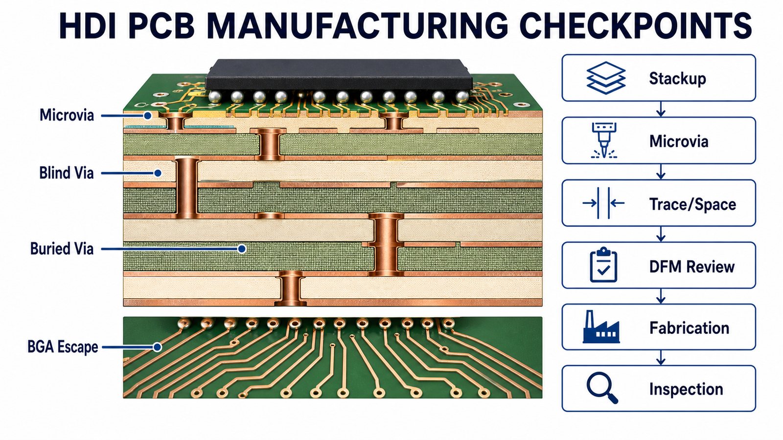
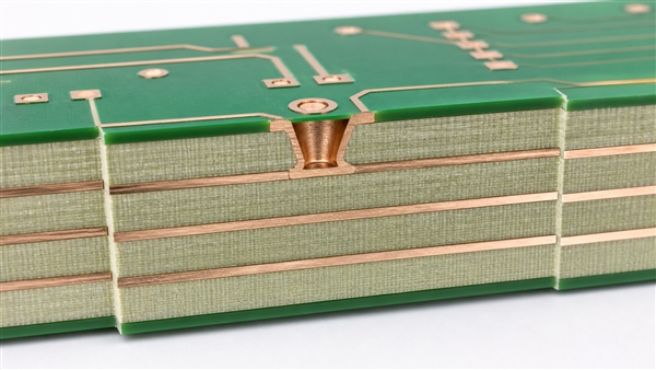
HDI PCB stackup decisions should be reviewed before quote approval because the via structure controls much of the manufacturing route. The buyer should identify whether the design uses laser microvias, blind vias, buried vias, stacked or staggered structures, via-in-pad or sequential buildup.
EBest Circuit’s verified process capability source includes laser buried/blind vias, mechanical blind/buried holes and special review conditions. It also shows that some HDI values depend on board type and supply route. For that reason, the safest public promise is not a universal number; it is a file-based review of the actual HDI stackup before quotation.
BGA Escape, Trace/Space and Routing Density Checks
BGA escape is one of the main reasons buyers look for an HDI PCB manufacturer. When pad pitch is tight, a through-hole via strategy may consume too much routing room. HDI routing can create a more compact path, but it must be checked against trace/space, annular ring, solder mask, laser via and registration limits.
For planning, EBest Circuit’s verified standard PCB data includes common 4/4mil line/space examples and special 3/3mil review conditions. FPC and rigid-flex HDI data also includes tighter project-specific examples. These are not automatic approvals; send the files so the actual BGA escape and layer structure can be reviewed.
HDI PCB Fabrication Process at a Glance
HDI PCB fabrication normally follows a tighter review path than standard PCB manufacturing. The process begins with file intake and stackup review, then moves through material confirmation, imaging, drilling or laser via formation, plating, lamination, solder mask, surface finish, routing, electrical test and inspection.
The exact route depends on the HDI structure. A simple HDI build may be reviewed differently from an any-layer or rigid-flex HDI project. For related manufacturing details, see our HDI PCB fabrication guide, then send your current files for project-specific confirmation.
DFM Review Before HDI PCB Fabrication
DFM review is a hard buying requirement for HDI PCB fabrication because small geometry changes can affect yield, cost and build feasibility. The review should cover stackup, microvia structure, hole size, aspect ratio, registration, annular ring, trace/space, copper balance, solder mask clearance, via-in-pad, panelization and test coupons when required.
A useful HDI DFM review does not only say whether the board can be made. It should tell the buyer what needs confirmation, what may increase cost, and what must change before the first build. This is especially important when the design is moving from prototype into repeat production.
Materials, Copper and Surface Finish Choices for HDI Boards
HDI PCB material and finish choices should match electrical performance, lamination needs, solderability and assembly requirements. EBest Circuit’s verified standard PCB source includes FR4 low-Tg, mid-Tg and high-Tg material options, as well as surface finishes such as OSP, HASL, ENIG, immersion silver, immersion tin, ENEPIG and hard gold fingers.
For many HDI projects, material selection is tied to signal integrity, thermal behavior, reliability and BGA assembly. If the design uses high-speed signals or demanding lamination requirements, include the target material or stackup notes in the RFQ. For general material context, the FR4 PCB page can help buyers frame the starting point before HDI-specific review.
HDI PCB Inspection and Reliability Checks
Inspection planning should be defined before the HDI quote is approved. HDI designs may need electrical testing, visual inspection, dimensional checks, microsection review, AOI, X-ray for assembly, impedance checks or project-specific documentation depending on the product and risk level.
If the board includes fine-pitch BGA, via-in-pad or dense PCBA, test access and inspection should be planned with assembly in mind. Do not wait until the boards are fabricated to decide how the assembled HDI board will be verified.
What Determines HDI PCB Cost?
HDI PCB cost is driven by stackup complexity, microvia structure, material, line/space, drilling, lamination route, surface finish, inspection and assembly scope. A low unit quote can be misleading if it does not include DFM review, special via requirements, test scope or PCBA checks.
| Cost Driver | Why It Matters | RFQ Control Point |
|---|---|---|
| Stackup and HDI structure | Controls lamination and via process route | Provide stackup and via type notes |
| Microvia and blind/buried vias | Changes drilling, plating and inspection requirements | Mark via structure clearly in files |
| BGA escape and trace/space | Fine routing may require special review | Send BGA package and routing constraints |
| PCBA and testing | Assembly and test can exceed bare-board risk | Send BOM, CPL, test and fixture requirements early |
Prototype, Low-Volume and Production HDI PCB Planning
HDI PCB planning should connect prototype evidence with the next production stage. A first build should prove the stackup, microvia approach, BGA escape, solderability, inspection method and test access. Low-volume builds should confirm repeatability and procurement assumptions before a larger order.
When a design is still changing, document revision, stackup, BOM, CPL and test changes carefully. If the HDI board also needs assembly, combine fabrication review with PCBA planning early so component placement and test access are not treated as afterthoughts.
How to Compare HDI PCB Manufacturers
Compare HDI PCB manufacturers by engineering review depth, not only by online quote speed. A useful manufacturer should be able to discuss HDI structure, DFM risk, material selection, PCBA impact and inspection scope before order release.
| Check Item | What to Ask | Why It Matters |
|---|---|---|
| HDI structure review | Can they review microvia, blind/buried via and stackup before quote? | HDI feasibility depends on structure, not just layer count |
| DFM feedback | Will they identify trace/space, annular ring, mask and drill risks? | Small geometry issues can delay the first build |
| Assembly support | Can they check BOM, CPL, BGA orientation and test access? | HDI layout risk often continues into PCBA |
| Inspection scope | What test and documentation are included? | Quotes are not comparable without test scope |
| Next-stage planning | Can they support prototype, low-volume and repeat builds? | HDI decisions made early can affect production cost |
HDI PCB RFQ File Checklist
A complete HDI PCB RFQ package gives the manufacturer enough information to review the real board, not a simplified version of it. Send these files and notes when possible:
- Gerber or ODB++ files.
- Drill files, laser drill notes and via structure notes.
- Stackup, material preference, copper weight and surface finish.
- BGA package details, pitch and routing constraints.
- Controlled impedance or high-speed signal requirements if applicable.
- BOM, CPL, assembly drawing and test requirements for PCBA projects.
- Prototype, low-volume and production quantities.
- Inspection, documentation, packaging and target delivery requirements.
Why Put EBest Circuit on Your HDI PCB RFQ Shortlist?
EBest Circuit is worth adding early to your HDI PCB quote comparison because HDI success depends on review quality before fabrication begins. We can help buyers review stackup, microvias, blind/buried vias, BGA escape, fine traces, material fit, PCBA readiness and test scope.
Compared with a quote-only buying path, EBest Circuit gives engineering teams and sourcing teams a clearer way to control risk and cost before the order is placed. For any-layer or more complex HDI structures, see also our any-layer HDI PCB discussion and send the current files for project review.
FAQ About HDI PCB Manufacturers
What is an HDI PCB manufacturer?
An HDI PCB manufacturer fabricates high-density interconnect circuit boards that may use microvias, blind vias, buried vias, via-in-pad, fine traces and compact multilayer stackups. The manufacturer should review the stackup, DFM risk, material and inspection scope before quoting.
Is HDI PCB fabrication different from standard PCB fabrication?
Yes. HDI PCB fabrication usually needs closer stackup review, laser via or blind/buried via planning, tighter routing checks and more careful DFM review. Standard PCB fabrication may not require the same via structure or routing density controls.
What files are needed for an HDI PCB quote?
Send Gerber or ODB++, drill files, stackup, via notes, material preference, copper weight, surface finish, BGA package details, quantity and test requirements. For assembly, also send BOM, CPL and assembly drawings.
Does HDI PCB cost more than a standard PCB?
HDI PCB often costs more when the design requires microvias, blind/buried vias, tighter trace/space, special lamination, extra inspection or PCBA review. The exact cost depends on the files and manufacturing route, so quote comparison should use the same RFQ package.
Can EBest Circuit support HDI PCB manufacturing for overseas buyers?
Yes. EBest Circuit directly supports overseas buyers with HDI PCB manufacturing review, DFM feedback, RFQ planning and optional PCBA coordination. Send the files early so the manufacturing route and quote scope can be checked before order release.
Final Recommendation
Choose an HDI PCB manufacturer that reviews the stackup and via structure before quoting, not one that only gives a fast price. For high-density boards, the quote must match the real microvia, BGA, material, inspection and assembly risk.
If you are preparing an HDI PCB or HDI PCBA project, send your Gerber or ODB++ files, drill files, stackup, via notes, BOM, CPL, quantity, material preference, surface finish, test requirements and target delivery to sales@bestpcbs.com. EBest Circuit will review the files and help you build a clearer HDI PCB manufacturing quotation path.
You may also like



Tags: HDI PCB, pcb manufacturing, PCB Quote