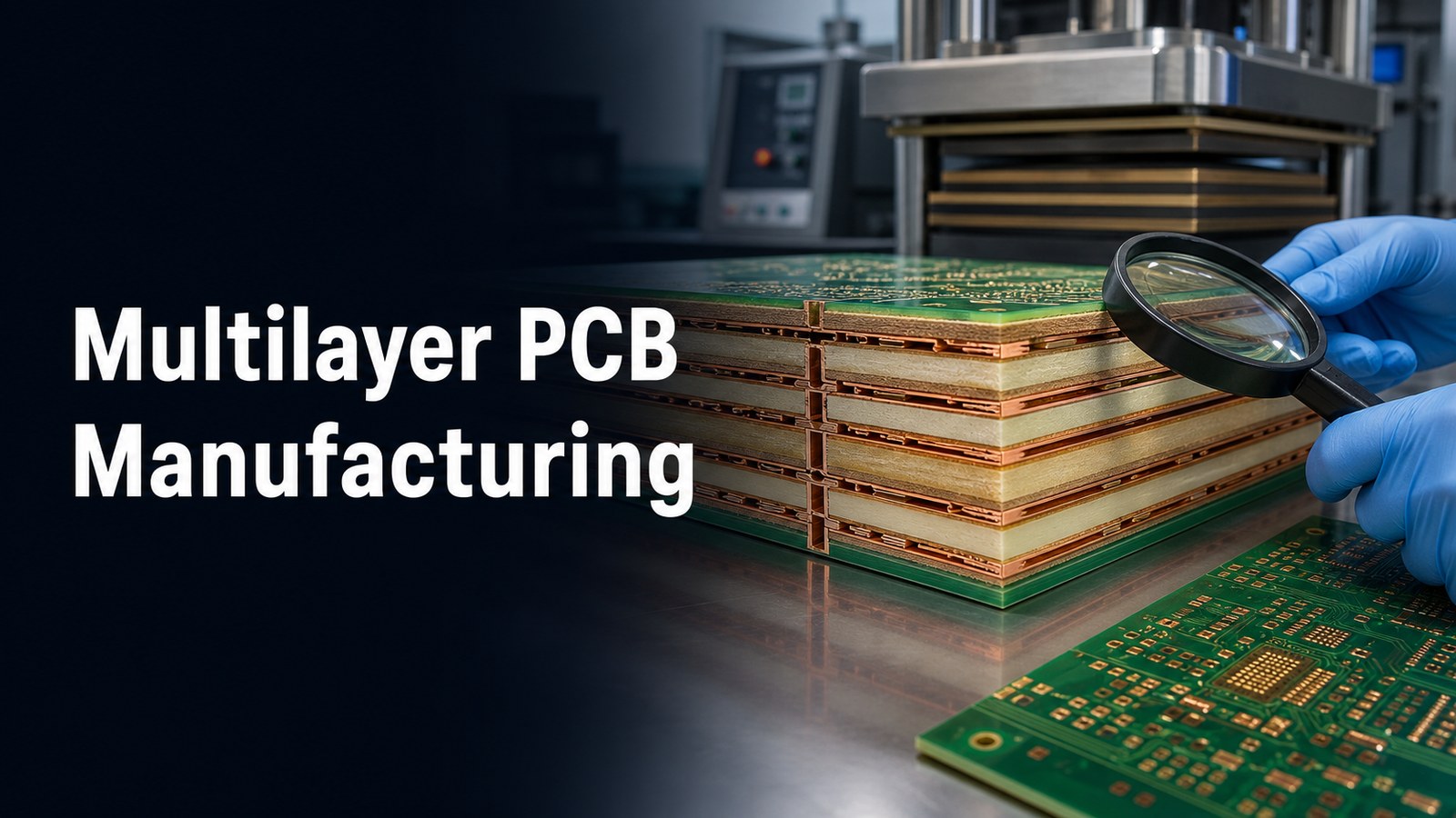
Multilayer PCB manufacturing builds circuit boards by stacking multiple copper layers with insulating core and prepreg materials, then laminating, drilling, plating and finishing the board so internal and external circuits connect reliably. It is used when a two-layer PCB cannot provide enough routing space, power distribution, signal integrity or compact layout.
This guide explains the multilayer PCB process, which design details affect manufacturability, and what buyers should include in an RFQ.
Multilayer PCB Manufacturing at a Glance
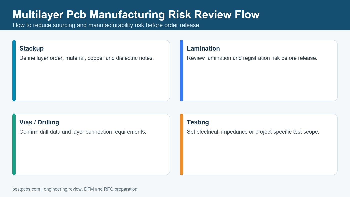
A multilayer PCB requires stackup control, lamination, drilling, plating, imaging, solder mask, surface finish, testing and documentation. Buyers should confirm layer count, stackup, material, copper, impedance, vias, finish and assembly needs before production.
| Area | What to confirm | Why it matters |
|---|---|---|
| Stackup | Layer order, cores, prepreg, copper and thickness | Controls routing, impedance, power planes and manufacturability. |
| Lamination | Material bonding, registration and thermal process | Poor lamination can affect reliability and internal connections. |
| Vias and drilling | Through vias, blind/buried vias if needed and drill tolerances | Defines how layers connect and how difficult the board is to build. |
| Testing | Electrical test, inspection and project-specific checks | Verifies internal and external circuit continuity before shipment. |
Is Your Multilayer PCB Project Being Delayed by Stackup or DFM Uncertainty?
Multilayer PCB buyers need early review because stackup, lamination, drilling, plating and test requirements become harder to correct after production starts.
| Customer Pain Point | Project Risk | How bestpcbs Helps |
|---|---|---|
| Stackup is not defined clearly | Layer order, dielectric thickness or impedance assumptions can cause redesign | bestpcbs asks for stackup drawings, material notes and impedance targets during RFQ review. |
| Via and drilling requirements are incomplete | Layer connections may become difficult or costly to manufacture | bestpcbs reviews drill files, via structure, annular rings and fabrication notes before release. |
| Assembly planning is delayed | Dense multilayer boards can have BGA, thermal or test access issues | bestpcbs checks BOM, CPL, assembly drawings and testing expectations together with fabrication files. |
| Testing scope is assumed | Internal layer problems can be hard to find without the right checks | bestpcbs confirms electrical, impedance or customer-defined test requirements before production. |
Buyer Priorities for Multilayer PCB Manufacturing
Multilayer PCB buyers should confirm stackup, lamination needs, via structure, drilling, plating, impedance, material, copper and test scope before production. Internal layers make early review more important because hidden problems are harder to correct after lamination.
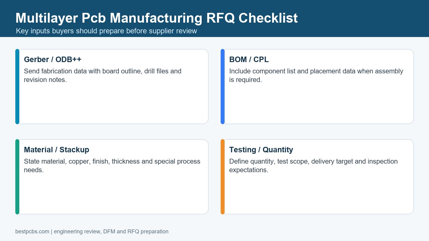
Prepare a clear stackup drawing, Gerber or ODB++ files, drill data, fabrication notes, impedance targets and assembly files when needed. A complete RFQ package helps the supplier review the real manufacturing risk instead of guessing from the layer count.
When Multilayer PCB Manufacturing Is Needed
Multilayer PCB manufacturing is needed when routing density, power planes, signal integrity, EMI control or board size requirements exceed what a single-sided or two-layer board can handle. It is common in communication equipment, industrial controls, medical electronics, embedded systems, high-speed boards and compact products.
If the design is still simple, review whether a double layer PCB manufacturing path is enough before increasing layer count.
Multilayer PCB Stackup Planning
Stackup planning should be agreed before fabrication because it affects impedance, thickness, material use, drilling and lamination risk. The supplier should not have to guess layer order from Gerber filenames.
- Define signal, power and ground layers.
- State total board thickness and copper requirements.
- Identify controlled impedance lines if applicable.
- Clarify material targets and special requirements.
- Label layer files clearly and include a fabrication drawing.
Multilayer PCB Manufacturing Process
The multilayer process usually includes inner layer imaging and etching, layup, lamination, drilling, plating, outer layer imaging, solder mask, surface finish, routing and testing. The exact process depends on layer count, material, via structure and inspection needs.
- Review Gerber or ODB++ files, stackup and fabrication notes.
- Create and inspect inner layer circuit patterns.
- Lay up cores and prepreg in the required layer order.
- Laminate the stack under controlled heat and pressure.
- Drill and plate holes to connect the required layers.
- Create outer layer circuits, solder mask, silkscreen and finish.
- Profile the board, run electrical test and package the finished PCBs.
Vias, Drilling and Layer Connections
Via structure is a major cost and manufacturability factor in multilayer PCB manufacturing. Standard through vias are simpler than blind or buried vias, while HDI structures require more controlled process planning.
If the design uses advanced via structures, compare it with the HDI PCB manufacturer RFQ guide and confirm what must be project-specific before quoting.
DFM Review Before Multilayer PCB Production
DFM review should happen before production because multilayer errors can be hidden inside the stack after lamination. Review drill-to-copper clearance, annular ring, copper balance, layer registration, impedance notes, solder mask, board outline and panelization.
The PCB design and manufacturing DFM guide is useful for preparing files before supplier review.
Materials, Copper and Surface Finish
Material, copper and finish choices should match the circuit performance, assembly process and operating environment. Standard FR-4 may be suitable for many multilayer boards, while high-speed, high-frequency, high-Tg or special materials may be needed for specific designs.
Do not state a special material or layer capability as final unless it is confirmed from current project data and supplier review.
Assembly Planning for Multilayer PCBs
Assembly planning should be considered during PCB design because dense multilayer boards often include fine-pitch components, BGAs, test access limits and thermal constraints. Fabrication and assembly files should be reviewed together when PCBA is required.
For assembled boards, prepare BOM, CPL, assembly drawing, polarity notes and testing requirements. The PCBA service path helps connect fabrication and assembly review.
Testing and Quality Control
Testing should verify internal connectivity, outer layer quality, dimensions, solderability and any customer-defined acceptance criteria. Multilayer boards need careful electrical test because faults can exist inside the board structure.
| Check | Purpose | Buyer input |
|---|---|---|
| Electrical test | Finds opens and shorts across layers | Netlist or accepted test scope |
| Impedance check | Verifies controlled impedance where required | Target values and stackup |
| AOI / visual inspection | Checks surface pattern, mask and assembly quality | Acceptance criteria and assembly files |
| Dimensional inspection | Confirms outline, slots and mounting fit | Fabrication drawing and tolerances |
What Determines Multilayer PCB Cost?
Multilayer PCB cost depends on layer count, stackup complexity, material, copper, board size, via structure, impedance control, finish, testing, quantity and assembly needs. The lowest quote may be incomplete if it assumes a simpler stackup or test scope.
For cost planning, compare the project with the custom PCB cost guide and ask suppliers to quote the same stackup.
RFQ Checklist for Multilayer PCB Manufacturing
A complete RFQ should let the supplier review stackup, manufacturability and testing before committing to price and lead time. This prevents delays caused by missing layer or drill information.
- Gerber or ODB++ files, drill files and fabrication drawing.
- Layer count, stackup, material, copper weight, thickness and surface finish.
- Controlled impedance, via type, special process or tolerance notes.
- BOM, CPL, assembly drawing and polarity notes if assembly is required.
- Quantity, prototype or production stage, target lead time and delivery destination.
- Electrical test, impedance test, inspection and packaging requirements.
Frequently Asked Questions About Multilayer PCB Manufacturing
What is a multilayer PCB?
A multilayer PCB has more than two conductive copper layers separated by insulating materials and connected through drilled and plated vias where required.
Is multilayer PCB manufacturing more expensive than two-layer PCB manufacturing?
Usually yes, because it requires stackup planning, inner layer processing, lamination, drilling, plating and more inspection. The exact cost depends on design complexity.
What files are needed for a multilayer PCB quote?
Send Gerber or ODB++, drill files, stackup, material notes, copper, thickness, finish, quantity and testing requirements. For assembly, also send BOM, CPL and assembly drawings.
Can bestpcbs help review multilayer PCB manufacturability?
Bestpcbs can review project files for PCB manufacturing and assembly questions. Exact layer, material and special process capability should be confirmed from current project data before order release.
Final RFQ Recommendation
Before ordering multilayer PCB manufacturing, make the stackup and via structure clear enough that the supplier can quote the real board. The more layers and special requirements a board has, the more important early DFM review becomes.
For a multilayer PCB quote, send your Gerber or ODB++ files, drill data, stackup, BOM, CPL, assembly drawing, quantity, material expectations, copper weight, surface finish, impedance notes, testing requirements and target lead time to sales@bestpcbs.com. The Best Technology / bestpcbs team can review the files and confirm what needs project-specific checking before production.