HDI PCB fabrication is the manufacturing process used to build high-density interconnect circuit boards with fine lines, laser microvias, blind vias, buried vias, via-in-pad structures, and sequential build-up layers. It is used when a conventional multilayer PCB cannot provide enough routing density, signal performance, or BGA escape space for compact electronics.
For engineers and sourcing teams, the right question is not only whether a factory can make an HDI PCB. The better question is whether the stackup, microvia structure, material choice, DFM review, inspection plan, and quotation data are mature enough for reliable production. EBest Circuit supports HDI PCB projects through PCB fabrication, DFM communication, prototype support, PCB assembly, component sourcing, and full turnkey manufacturing.
What Is HDI PCB Fabrication?
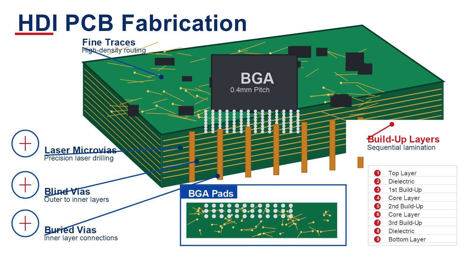
HDI PCB fabrication is a specialized PCB manufacturing flow for boards with higher wiring density than conventional through-hole multilayer PCBs. It usually combines fine copper patterning, laser drilling, blind and buried vias, sequential lamination, via plating, via filling, solder mask, surface finish, and electrical testing.
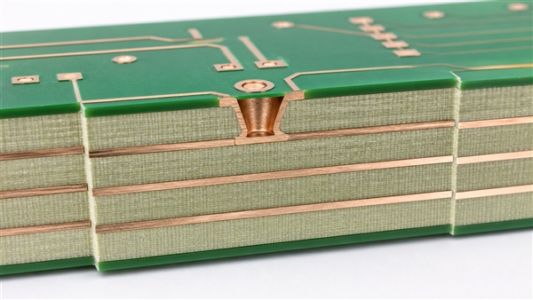
An HDI board may use blind microvias from an outer layer to an adjacent inner layer, buried vias between internal layers, or stacked and staggered microvias across build-up layers. These structures free routing channels under fine-pitch components and reduce the space consumed by large mechanical through-holes.
HDI fabrication is commonly used in communication modules, medical electronics, compact industrial controls, automotive electronics, cameras, wearable devices, IoT products, high-speed boards, and products using fine-pitch BGA or CSP packages.
When Is HDI Better Than a Standard Multilayer PCB?
HDI becomes useful when component density, routing escape, board size, or electrical performance makes a standard multilayer PCB inefficient. It should be chosen for a real design reason, not simply because it sounds more advanced.
| Design situation | Why HDI may help | Engineering or sourcing note |
| Fine-pitch BGA or CSP packages | Microvias can help escape dense component pins with less layer congestion. | Confirm BGA pitch, via-in-pad rules, target pad size, and via filling early. |
| Very compact enclosure | HDI can increase routing density without increasing board area. | Compare HDI cost against a larger standard PCB before the mechanical design is frozen. |
| High-speed or RF routing | Shorter transitions and controlled stackups can support cleaner signal paths. | Ask for impedance stackup review and material confirmation before layout release. |
| High I/O count components | Blind and buried vias create more routing channels under dense packages. | Review drill maps, layer transitions, and lamination cycles with the fabricator. |
| Prototype routing failure | HDI may solve routing blockage without adding many conventional layers. | Use DFM review before assuming a more complex stackup is the only solution. |
BestPCBs HDI PCB Fabrication Capability Snapshot
For a quotation-ready HDI project, capability should be discussed with the actual stackup, copper weight, material, panel size, quantity, and reliability target. The following values summarize useful starting points from EBest Circuit’s current PCB process capability data.
| Capability area | Available range or support | Buyer note |
| Layer count | Standard FR4: 1-10 layers; special multilayer FR4: 10-32 layers. | Boards with 8 layers or more should use high-Tg material. |
| Laser blind / buried vias | 0.10 mm laser blind/buried via capability. | Useful for HDI build-up layers and fine-pitch component escape. |
| Finished hole diameter | Standard minimum finished hole: 0.20 mm; special process: 0.15 mm. | Mechanical blind/buried holes can also be reviewed down to 0.15 mm by special process. |
| Line width and spacing | Standard 1 oz inner/outer layer: 4/4 mil; special process can review 3/3 mil for 1 oz and 1/2 oz cases. | Heavy copper requires wider line and spacing rules. |
| Copper thickness | Standard FR4 copper: 0.5 oz to 5 oz; special process: 5 oz to 20 oz. | High-current HDI designs need early copper balance and plating review. |
| Surface finishes | OSP, HASL, lead-free HASL, ENIG, immersion silver, immersion tin, ENEPIG, hard gold fingers, ENIG+OSP, and ENIG+hard gold fingers. | Choose based on BGA assembly, shelf life, bonding, solderability, and contact wear. |
These values are practical starting points, not a substitute for design review. A 3/3 mil line-space area, a 0.15 mm hole, or a 32-layer board should be checked against the actual copper weight, stackup, material, impedance requirement, and production quantity.
HDI Stackup Types and Via Structures
The HDI stackup defines how many build-up layers are added to the core and how microvias connect those layers. The choice affects routing density, lamination cycles, registration control, cost, and reliability.
| Structure | Typical use | Manufacturing impact |
| 1+N+1 HDI | Moderate HDI density and fine-pitch component escape. | Usually simpler and more economical than multi-step HDI build-up. |
| 2+N+2 HDI | Higher routing density and more complex BGA escape. | Requires more sequential lamination control and tighter registration review. |
| Blind microvia | Connects an outer layer to an adjacent inner layer. | Usually laser drilled and plated; depth, diameter, and target pad must be reviewed. |
| Buried via | Connects internal layers without reaching the outer layers. | Requires internal drilling and plating before later lamination. |
| Stacked microvia | Connects build-up layers vertically in the same position. | Often requires copper filling and stronger reliability review. |
| Staggered microvia | Offsets microvias between layers. | Can reduce some stacked-via stress risk but uses more routing area. |
EBest Circuit’s HDI product page discusses 1+N+1, 2+N+2, and every-layer interconnection structures. In a real project, the final structure should be selected by BGA pitch, I/O count, routing density, impedance needs, and reliability target.
HDI PCB Fabrication Process
The HDI PCB fabrication process starts with engineering review and moves through inner-layer processing, lamination, laser drilling, copper plating, via filling, outer-layer patterning, solder mask, surface finish, and final testing.
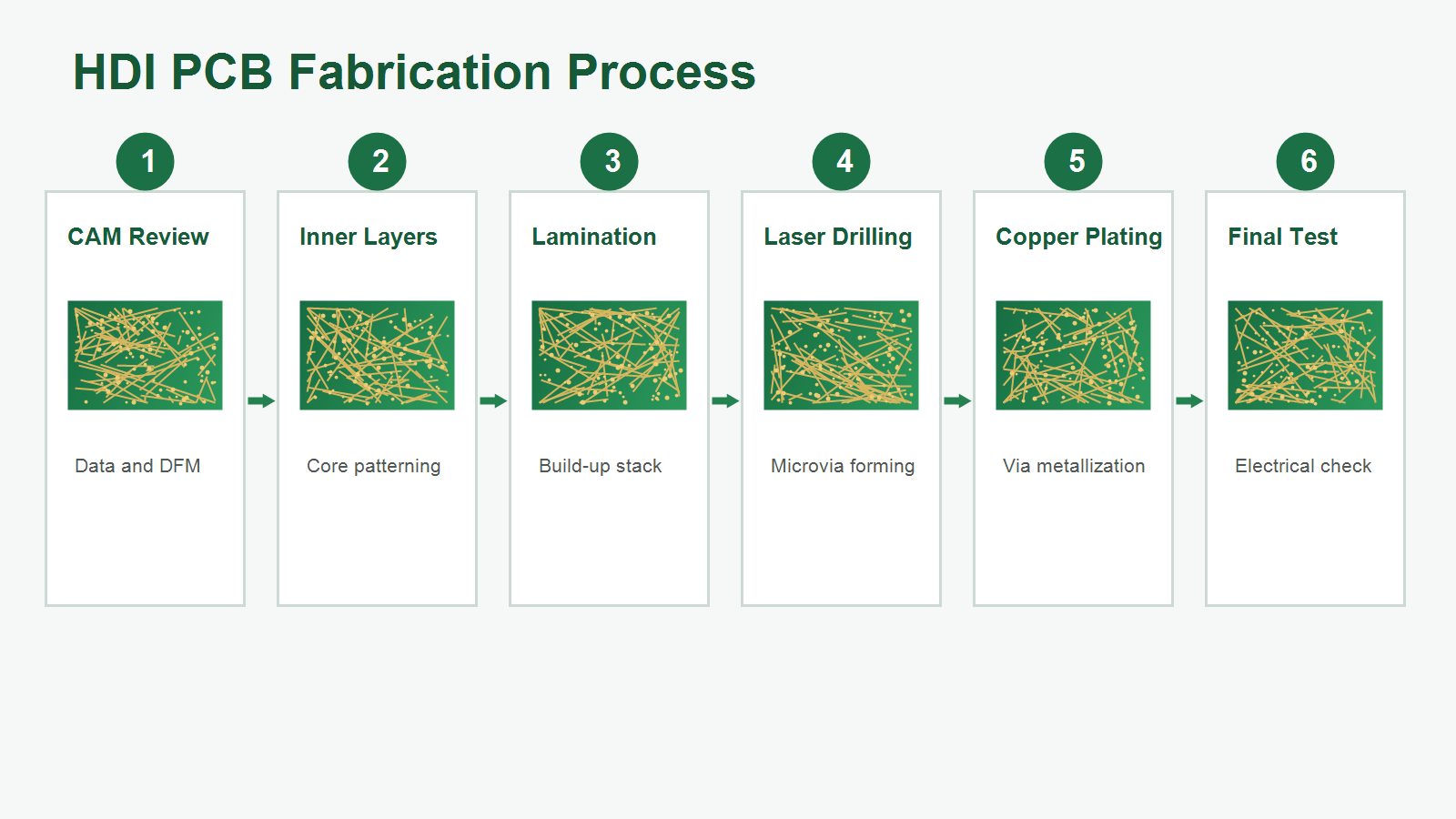
- CAM and DFM review: Check Gerber or ODB++ data, stackup, drill map, impedance notes, copper spacing, annular rings, via structures, and panelization.
- Inner-layer imaging and etching: Pattern internal copper layers and inspect them before they are buried inside the stack.
- Buried via processing: Drill, plate, and inspect internal vias where the HDI stackup requires them.
- Sequential lamination: Add build-up dielectric and copper layers in controlled lamination cycles.
- Laser drilling: Form microvias between adjacent layers for dense interconnect routing.
- Desmear and via preparation: Prepare the via surface for reliable copper deposition.
- Copper plating and via filling: Build conductive via walls and fill or cap vias when required by via-in-pad or stacked structures.
- Outer-layer imaging and etching: Define fine outer copper features and inspect for opens, shorts, and spacing issues.
- Solder mask and surface finish: Apply solder mask and finish pads with ENIG, ENEPIG, OSP, immersion silver, immersion tin, or another specified finish.
- Final inspection and test: Use AOI, electrical test, impedance test, microsection review, dimensional inspection, and final visual inspection where required.
Design Rules That Affect HDI Manufacturability
HDI manufacturability depends on whether the layout respects the fabricator’s real line width, spacing, pad, via, dielectric, copper, solder mask, and registration limits. Small design-rule changes can strongly affect yield, cost, and lead time.
- Keep laser microvias within the manufacturer’s recommended diameter, depth, and layer-span limits.
- Avoid stacked microvias unless routing density or electrical constraints truly require them.
- Use via-in-pad only when it solves a fine-pitch component escape or assembly problem.
- Confirm whether BGA pads require filled and capped vias to prevent solder wicking.
- Use relaxed trace and space rules outside dense routing areas when possible.
- Review copper balance to reduce lamination distortion and registration risk.
- Define controlled impedance with stackup, tolerance, reference plane, and coupon requirements.
- Send early BGA escape and placement data for DFM review before completing the full layout.
For dense products, the best workflow is collaborative. The PCB designer, fabricator, and assembler should review BGA escape, stackup, via filling, surface finish, and assembly process before the design is frozen.
Microvia Reliability Risks and How to Reduce Them
Microvia reliability depends on geometry, plating quality, via filling, material behavior, thermal stress, and the number of stacked levels. Common risks include voiding, weak target-pad connection, plating cracks, solder wicking, and registration misalignment.
| Risk | Possible cause | Prevention or inspection point |
| Microvia voiding | Incomplete filling or unstable plating control. | Request microsection evidence and via fill confirmation. |
| Target pad separation | Thermal stress or poor metallurgical connection at the via base. | Review microvia geometry, material CTE, and thermal cycling requirements. |
| Stacked via fatigue | Multiple stacked levels increasing local stress. | Use staggered vias where possible or confirm copper-filled stacked via reliability. |
| Solder wicking in via-in-pad | Unfilled or poorly capped via inside a component pad. | Specify filled and capped via-in-pad for BGA pads when required. |
| Registration misalignment | Sequential lamination movement and tight pad geometry. | Use realistic capture pads and review layer-to-layer registration capability. |
Materials and Surface Finishes for HDI Boards
HDI material and surface finish choices should match signal speed, thermal stress, soldering process, storage, reliability target, and cost. Standard FR4 may be suitable for many HDI boards, while high-speed, RF, high-temperature, or reliability-sensitive applications may need higher-performance laminates.
EBest Circuit’s material capability includes FR4 low-Tg, mid-Tg, high-Tg, halogen-free options, and special materials such as Isola, Rogers, Nelco, Taconic, PTFE, and other high-performance laminates when project requirements justify them. Surface finish options include OSP, HASL, lead-free HASL, ENIG, immersion silver, immersion tin, ENEPIG, hard gold fingers, ENIG+OSP, and ENIG+hard gold fingers.
| Choice | Where it matters | Practical note |
| High-Tg FR4 | Multilayer and reliability-sensitive HDI products. | Use for 8-layer and above FR4 projects and applications with higher thermal stress. |
| Low-loss laminate | High-speed, RF, antenna, and communication designs. | Confirm Dk, Df, copper profile, impedance model, and availability before layout release. |
| Thin dielectric build-up layer | Laser microvia formation and compact layer transitions. | Microvia depth and target pad geometry must match the fabricator’s capability. |
| ENIG or ENEPIG | BGA assembly, fine-pitch pads, contact reliability, and wire bonding in some designs. | Choose based on assembly process, shelf life, bonding needs, and reliability requirement. |
| OSP, immersion silver, or immersion tin | Cost-sensitive or process-specific applications. | Review storage, handling, solderability, and assembly window with the assembler. |
Quality Control and Testing for HDI PCB Fabrication
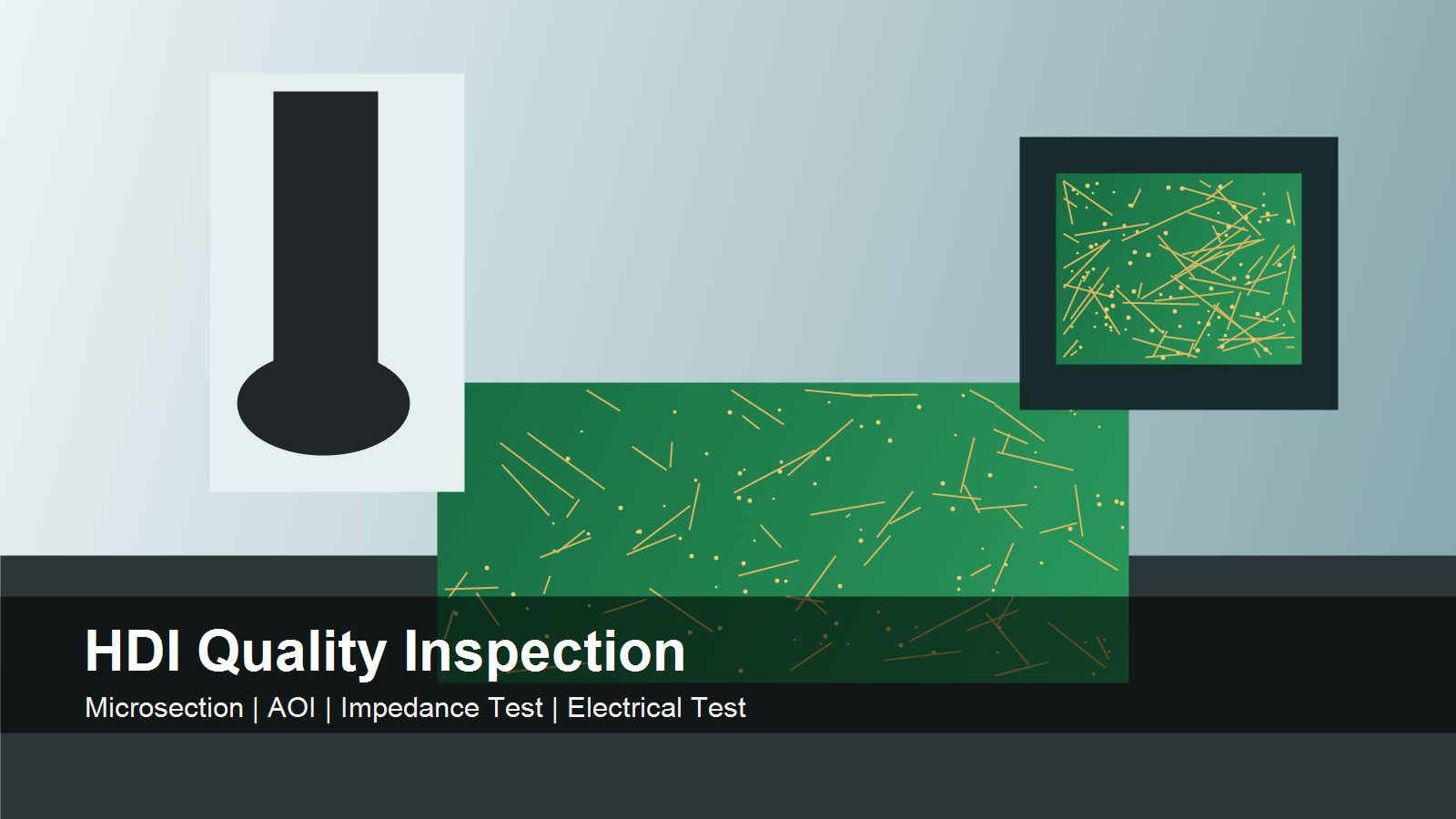
HDI quality control must verify both visible board quality and hidden interconnect reliability. Microvias and buried vias are not fully visible after lamination, so inspection must include structural evidence and process control, not only final appearance.
- CAM and DFM review: catches manufacturability risk before production.
- Inner-layer AOI: checks opens, shorts, over-etching, and spacing defects before lamination.
- Laser via inspection: verifies microvia opening, position, and target pad relationship.
- Microsection: verifies via wall quality, plating thickness, filling, target-pad connection, and lamination structure.
- Impedance test: checks controlled impedance structures using coupons when specified.
- Electrical test: confirms continuity and isolation before shipment or assembly.
- Final visual and dimensional inspection: checks outline, solder mask, finish, legend, and workmanship.
HDI PCB Fabrication Cost Drivers
HDI PCB cost is driven by build-up complexity, lamination cycles, microvia structure, material choice, line and space requirements, via filling, surface finish, testing, and yield risk. A lower unit price is not always the lower project cost if it causes redesign, scrap, assembly defects, or reliability failure.
| Cost driver | Why it changes cost | How to control it |
| Sequential lamination cycles | More build-up cycles add process time, handling, registration risk, and cost. | Use the simplest stackup that meets routing and reliability needs. |
| Stacked microvias | They often need tighter process control and copper filling. | Use staggered vias where layout allows. |
| Via-in-pad filling | Filling, capping, and planarization add process steps. | Apply via-in-pad only where it solves dense component escape or assembly needs. |
| Fine line and space | Very fine copper features reduce process margin. | Use 3/3 mil only where the dense area truly needs it. |
| Special laminates | Low-loss or high-temperature materials increase material and handling cost. | Match material to actual electrical and thermal requirements. |
| Testing requirements | Impedance coupons, microsections, and reliability checks add time and evidence cost. | Specify the tests needed for the application risk level. |
What Files Are Needed for an HDI PCB Quote?
An accurate HDI PCB quote needs more than Gerber files. The supplier needs enough fabrication, stackup, material, via, finish, tolerance, and testing information to judge manufacturability and avoid hidden assumptions.
- Gerber, ODB++, IPC-2581, or complete fabrication data.
- NC drill files and drill map showing mechanical holes, blind vias, buried vias, and laser microvias.
- Layer stackup with dielectric thickness, copper weight, material type, and controlled impedance notes.
- Board outline, dimensions, tolerance, panelization, and routing notes.
- Surface finish requirement, such as ENIG, ENEPIG, OSP, immersion silver, or immersion tin.
- Via filling, capping, plugging, and via-in-pad requirements.
- Solder mask color, legend color, UL or marking requirements if applicable.
- Impedance control requirements and test coupon expectations.
- IPC class, reliability, thermal cycling, automotive, medical, or compliance requirements if specified.
- Quantity, prototype or mass production stage, delivery target, BOM, and assembly plan if PCBA is included.
How to Choose an HDI PCB Manufacturer
A capable HDI PCB manufacturer should explain the manufacturing trade-offs for your exact layout, not only list broad capability numbers. The supplier should review the stackup, microvia structure, material, via filling, inspection plan, and assembly needs before production.
Ask these questions before placing an HDI order:
- Does the design fit standard FR4 production, or does it need special 10-32 layer review?
- Can the laser blind/buried via structure use the 0.10 mm process safely with the selected dielectric?
- Does the BGA escape require 3/3 mil special line/space or via-in-pad review?
- Are filled and capped vias required under BGA pads?
- What microsection evidence can be provided for first article approval?
- How will impedance be calculated, built, and tested?
- Which surface finish is recommended for the assembly process and shelf-life requirement?
- Which requirements are standard process and which need special process review?
EBest Circuit supports HDI PCB projects with DFM communication, PCB fabrication, component sourcing, assembly, testing, and turnkey manufacturing. For HDI capability details, see the HDI PCB product page, the PCB capability page, and related PCB assembly services.
FAQ
What does HDI mean in PCB fabrication?
HDI means high-density interconnect. In PCB fabrication, it refers to boards built with denser routing features such as fine lines, smaller vias, blind vias, buried vias, and laser-drilled microvias.
Is HDI PCB fabrication the same as multilayer PCB fabrication?
No. HDI boards are multilayer boards, but they add specialized processes such as sequential lamination, laser drilling, microvia plating, and sometimes via filling and capping.
What is the minimum laser via size for BestPCBs HDI fabrication?
EBest Circuit’s current capability data lists 0.10 mm laser blind/buried via capability. The final approval depends on dielectric thickness, layer span, copper weight, pad geometry, and production quantity.
Can BestPCBs support 3/3 mil line width and spacing?
For 1 oz and 1/2 oz cases, special process review can reach 3/3 mil line width and spacing. Heavy copper designs require wider rules, so final approval should be checked with the stackup and copper thickness.
What is the difference between blind vias and buried vias?
A blind via connects an outer layer to an inner layer without passing through the whole board. A buried via connects only internal layers and is hidden after lamination.
Are stacked microvias reliable?
Stacked microvias can be reliable when the geometry, copper filling, plating process, material, and inspection controls are appropriate. For high-reliability products, review stacked versus staggered microvias during DFM.
Why is via-in-pad used in HDI PCB fabrication?
Via-in-pad is used when dense components, especially fine-pitch BGAs, do not leave enough room for traditional fanout routing. The via usually needs filling and capping to prevent solder wicking.
Which surface finish is best for HDI PCB fabrication?
There is no single best finish for every HDI board. ENIG is common for fine-pitch assembly, while ENEPIG, OSP, immersion silver, immersion tin, and hard gold options may fit different assembly and reliability needs.
Does HDI always reduce PCB cost?
No. HDI can reduce board size or layer count in some designs, but it also adds process cost. The total cost depends on whether the routing-density benefit offsets lamination, laser drilling, via filling, and inspection cost.
What is the biggest risk in HDI PCB fabrication?
The biggest risk is hidden interconnect reliability around microvias, plating, filling, and target-pad connection. DFM review, process control, microsection inspection, and realistic stackup choices reduce this risk.
Can HDI PCBs support high-speed signals?
Yes. HDI PCBs can support high-speed signals when the stackup, impedance control, material, return path, via structure, and fabrication tolerances are designed correctly.
What should I send for an HDI PCB quote?
Send Gerber or ODB++ files, drill files, stackup, material request, copper weight, impedance notes, via filling requirements, surface finish, quantity, delivery target, and assembly information if PCBA is included.
Final Takeaway
HDI PCB fabrication is valuable when compact size, fine-pitch components, high routing density, or signal requirements make standard multilayer routing inefficient. The best results come from early stackup planning, realistic microvia choices, material confirmation, DFM review, and supplier evidence rather than late-stage price shopping.
If you are evaluating an HDI PCB fabrication project, EBest Circuit can support PCB manufacturing, DFM review, component sourcing, assembly, testing, prototype builds, and production planning. Send your Gerber files, stackup, drill files, quantity, and assembly requirements to sales@bestpcbs.com for engineering review and quotation support.
You may also like





Tags: HDI PCB, microvias, pcb fabrication, pcb manufacturing