

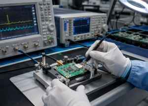
Looking for IoT PCB assembly turnkey service that can move smart hardware from prototype to production with fewer risks? IoT products often combine compact PCB layouts, wireless modules, sensors, power circuits, connectors, and functional testing requirements. A reliable turnkey PCBA partner helps reduce sourcing gaps, assembly errors, rework, and delivery uncertainty.
A complete IoT PCB assembly turnkey service brings PCB fabrication, component sourcing, SMT assembly, through-hole assembly, inspection, testing support, and delivery into one controlled workflow. This article explains service scope, product types, required files, process steps, quality control, delivery support, and how EBest supports IoT access control PCB, wireless modules, sensor boards, and industrial IoT PCBA projects.
What Is IoT PCB Assembly Turnkey Service?
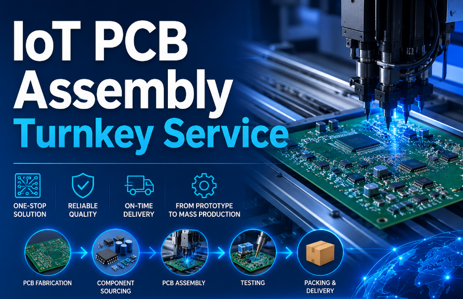
IoT PCB assembly turnkey service is a one-stop PCBA solution for connected electronic products. It covers PCB fabrication, component sourcing, SMT assembly, through-hole assembly, mixed assembly, inspection, testing support, and delivery through one coordinated production flow.
This service is widely used for smart home devices, IoT access control PCB products, wireless sensor boards, industrial IoT modules, gateways, monitoring equipment, and asset tracking devices. These products usually require stable wireless communication, reliable power control, compact placement, and consistent batch quality.
The main advantage of IoT PCB assembly turnkey service is easier project management. Instead of coordinating bare boards, components, soldering, and inspection through separate suppliers, the full PCBA process can be managed through one production partner. This reduces communication gaps and lowers the risk of mismatch between PCB layout, BOM data, component packages, and assembly requirements.
For connected devices, PCBA quality directly affects signal stability, power reliability, operating life, and field performance. A weak assembly process can turn a promising product into a delayed or unreliable launch. That is why choosing a reliable IoT PCBA turnkey solution matters from sample validation to repeat production.
What Does an IoT PCB Assembly Turnkey Service Include?
An IoT PCB assembly turnkey service usually includes everything required to turn approved PCB files and component data into finished IoT PCB assemblies. The goal is to keep PCB production, component preparation, assembly, inspection, and delivery under one organized workflow instead of splitting the project across several separate vendors.
A typical IoT PCB assembly turnkey service project may include:
- PCB manufacturing preparation
The process starts with production files, board specifications, stack-up requirements, surface finish, copper weight, solder mask details, and panel requirements. For IoT products, this step helps confirm whether the board is suitable for compact components, RF sections, connectors, and power circuits. - BOM review and component preparation
The BOM is checked for part numbers, package types, values, quantities, polarity, and approved alternatives. This helps reduce the risk of wrong parts, unavailable components, and last-minute sourcing issues before assembly starts. - Component sourcing and kitting
Components can be prepared according to the approved BOM, including ICs, passive components, connectors, modules, sensors, relays, and power devices. Proper kitting helps keep the SMT and through-hole assembly process more stable. - SMT assembly
Surface-mounted components are assembled through solder paste printing, placement, reflow soldering, and inspection. This step is important for IoT boards with dense layouts, fine-pitch packages, wireless modules, and small passive components. - Through-hole and mixed assembly
Connectors, terminals, relays, switches, transformers, and other plug-in components may require through-hole soldering. Many IoT boards use mixed assembly, combining SMT parts with stronger mechanical or power-related components. - BGA, QFN, and fine-pitch assembly support
IoT control boards, gateways, and wireless modules may include BGA, QFN, QFP, or other fine-pitch packages. These components require accurate placement, controlled soldering, and suitable inspection methods. - Inspection and testing support
Inspection may include visual checking, AOI, X-ray inspection for hidden joints, continuity checks, power-on testing, and functional test support. Testing requirements should be confirmed before production so the finished PCBA matches the intended application. - Final checking, packing, and delivery
Finished boards are checked for appearance, quantity, labels, packing method, and order consistency before shipment. This helps protect the assembled boards during transport and reduces problems after arrival.
For IoT access control PCB, smart sensor boards, wireless gateways, and monitoring devices, this full-service model helps reduce project handoff risk. It also makes the path from prototype builds to repeat production easier to manage.
What Types of IoT Products Use Turnkey PCB Assembly?
IoT PCB assembly turnkey service is suitable for IoT products that require stable hardware performance, reliable component sourcing, compact assembly, and repeatable production quality. These products often collect data, control equipment, connect to cloud platforms, or communicate with other smart devices.
Common product types include:
- IoT access control PCB for smart locks, access terminals, card readers, relay control boards, and smart entry systems.
- Smart home devices such as thermostats, lighting controllers, security sensors, smart switches, and home gateways.
- Wireless sensor modules for temperature, humidity, motion, pressure, vibration, gas detection, and environmental monitoring.
- Industrial IoT devices for machine monitoring, automation control, remote diagnostics, and equipment data collection.
- Asset tracking devices using GNSS, Bluetooth, LTE, NB-IoT, LoRa, UWB, or other wireless technologies.
- Smart monitoring systems for energy systems, agriculture, logistics, healthcare equipment, and building control.
- Gateway and communication modules that connect sensors, edge devices, local networks, and cloud platforms.
These products require more than basic soldering. They require package matching, RF awareness, power stability, inspection discipline, and consistent production records. A well-managed turnkey IoT PCB assembly process helps reduce uncertainty across prototype builds, pilot runs, and repeat production.
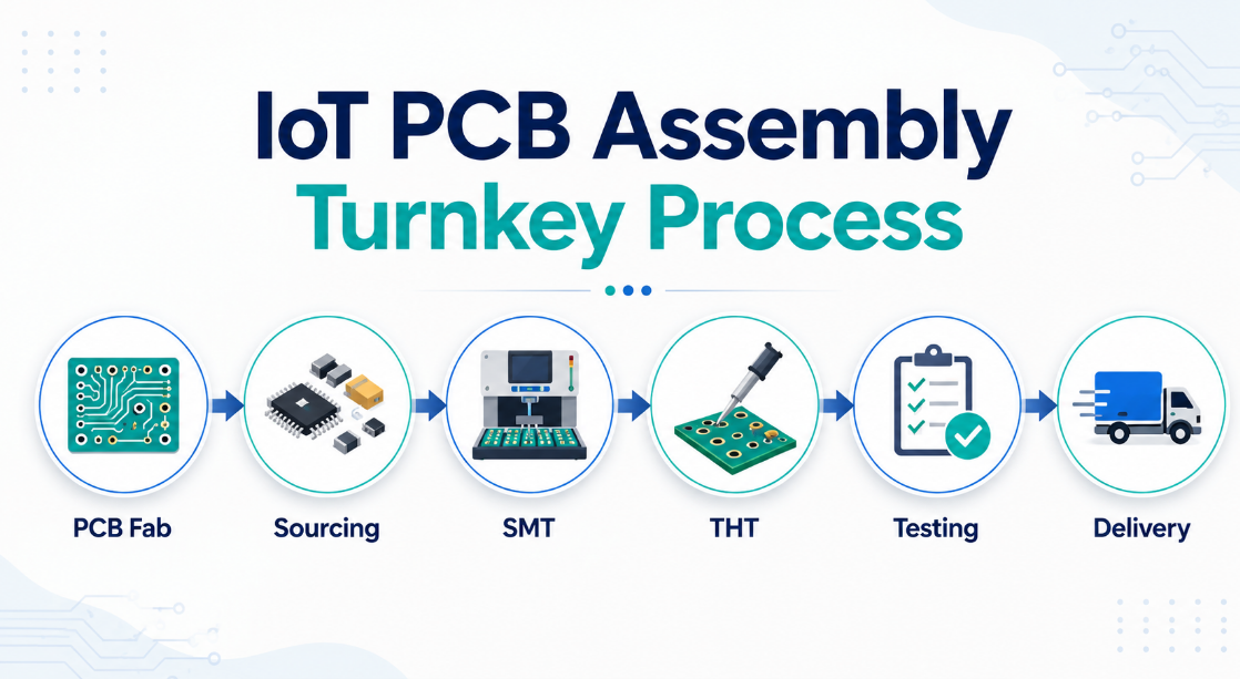
What Is the IoT PCB Assembly Turnkey Process?
The IoT PCB assembly turnkey service process should be clear, traceable, and easy to manage. A structured process reduces file errors, component mismatches, soldering defects, inspection gaps, and delivery uncertainty. It also helps the project move smoothly from prototype validation to mass production.
1. Project file review
Gerber files, BOM, CPL, assembly drawings, testing notes, and special requirements are reviewed before production starts.
2. DFM and assembly risk check
Footprint matching, component polarity, spacing, fiducials, panel format, soldering risk, and placement direction are checked.
3. PCB fabrication
Bare boards are produced according to material, layer count, copper weight, board thickness, surface finish, solder mask, and tolerance requirements.
4. Component sourcing
Components are prepared based on approved BOM data, manufacturer part numbers, package details, quantities, and substitute rules.
5. SMT assembly
Solder paste printing, component placement, reflow soldering, and AOI inspection are completed for surface-mounted components.
6. Through-hole assembly
Connectors, terminals, relays, switches, transformers, and other plug-in components are assembled with suitable soldering methods.
7. Inspection and testing
AOI, visual inspection, X-ray inspection for hidden joints, and functional testing support are arranged based on project requirements.
8. Final checking and packing
Finished IoT PCB assemblies are checked, labeled, protected with proper packing, and prepared for delivery.
This process applies to IoT sensor PCB assembly, IoT module PCB assembly, IoT access control PCB assembly, smart device PCBA, and industrial IoT PCB assembly projects. Each step should be confirmed before the next stage begins, especially when the board includes RF modules, power control, or safety-related functions.
What Files Are Required for an IoT PCB Assembly Turnkey Quote?
Complete files help the project review move faster and more accurately. For an IoT PCB assembly turnkey service quote, unclear files can cause wrong component selection, assembly delays, polarity mistakes, testing gaps, or repeated confirmation before production.
The main files include:
- Gerber files for PCB fabrication.
- BOM file with reference designator, value, package, quantity, manufacturer part number, and approved alternatives.
- CPL or pick-and-place file for SMT component position and rotation.
- Assembly drawing showing polarity, connector direction, special components, and placement notes.
- PCB specification including material, board thickness, copper weight, surface finish, solder mask color, and impedance requirements.
- Testing instructions for power-on checks, communication verification, programming, or functional testing.
- Panel requirements for assembly panel size, breakaway tabs, tooling holes, fiducials, and handling rules.
- Sample photos or previous version files when the project is based on an existing IoT PCBA.
For IoT access control PCB projects, extra details can make the review more accurate. These may include relay control requirements, power input range, lock control notes, connector details, communication interfaces, and test procedures. Clear files give production teams a stronger starting point and help reduce avoidable production risk.
What Should Be Checked Before IoT PCB Assembly Starts?
Before IoT PCB assembly starts, key production details should be confirmed carefully. IoT boards are often compact and function-heavy, so a small error in polarity, package selection, RF clearance, or connector direction can affect the final device.
Important checks include:
- BOM accuracy: part number, value, package, tolerance, voltage rating, and substitute rules.
- Component polarity: diode, LED, IC, capacitor, connector, module, and relay direction.
- Footprint matching: PCB pad size and actual component package compatibility.
- RF section clearance: antenna keep-out area, shielding area, grounding, and impedance-sensitive sections.
- Power circuit reliability: regulator rating, fuse selection, surge protection, current load, and thermal behavior.
- Connector alignment: housing fit, cable direction, terminal position, and mechanical clearance.
- Testing access: test points, programming pads, power input points, and communication interfaces.
- Panel requirements: board spacing, tooling holes, fiducials, breakaway tabs, and assembly handling.
These checks are especially important for IoT access control PCB assembly because the same board may manage locks, readers, relays, power modules, and wireless communication. When these details are confirmed early, the PCBA process becomes more predictable and easier to scale.
What Are Common Challenges in IoT PCB Assembly Turnkey Projects?
IoT PCB assembly turnkey service projects often involve more variables than standard PCBA orders. Wireless modules, sensors, fine-pitch ICs, connectors, battery circuits, PoE circuits, and mixed assembly components may all appear on one compact board. Without early review, these details can create performance and delivery risks.
Common challenges include:
- Component availability changes
IoT products often use MCUs, wireless modules, sensors, memory chips, and power ICs. Approved substitutes should be discussed early so production can continue smoothly if the original part becomes unavailable. - RF signal instability
Wi-Fi, Bluetooth, GNSS, LoRa, NB-IoT, LTE, and UWB modules may be affected by poor antenna clearance, weak grounding, shielding problems, or contamination near RF sections. - Fine-pitch soldering defects
BGA, QFN, QFP, 01005 components, and dense SMT layouts require accurate placement, stable solder paste printing, controlled reflow, AOI, and X-ray inspection when hidden joints are involved. - Power and thermal concerns
Battery-powered IoT devices, PoE boards, access control systems, and relay-control circuits may face voltage drop, current surge, heat buildup, or connector overload. - Testing gaps
Some IoT PCBA projects require firmware programming, power-on testing, communication checks, relay action checks, and sensor response verification before delivery. - Prototype-to-production differences
A prototype may pass basic validation, but larger production can expose sourcing, panelization, soldering, packing, or testing consistency issues.
A reliable IoT PCB assembly turnkey service should not only assemble the board but also help identify production risks before they become repeated problems. This is where early file review, component confirmation, inspection control, and clear testing instructions become valuable.
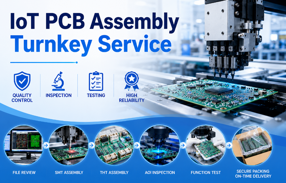
How Does EBest Control Quality for IoT PCB Assembly Orders?
EBest controls IoT PCB assembly quality from file review to final shipment, helping reduce assembly errors, rework, delivery risk, and batch inconsistency for IoT products.
- File review before production
EBest reviews Gerber files, BOM, CPL, assembly drawings, polarity marks, panel requirements, and testing notes before production starts. This helps identify missing data, footprint mismatches, unclear placement direction, and assembly risks before they affect production. - PCB fabrication control
EBest checks PCB material, board thickness, copper thickness, solder mask, surface finish, hole quality, and board appearance. For IoT access control PCB and wireless IoT boards, stable PCB quality supports reliable power, signal, and mechanical performance. - Component verification
EBest checks component package, value, quantity, polarity, and approved substitute status before assembly. This reduces the risk of wrong parts, unavailable components, or package mismatch in turnkey PCBA projects. - SMT process control
EBest controls solder paste printing, placement accuracy, reflow soldering, and AOI inspection during SMT assembly. This helps reduce solder bridging, tombstoning, shifted components, missing parts, and poor solder joints on compact IoT PCBA. - BGA and fine-pitch inspection
For BGA, QFN, QFP, and fine-pitch components, EBest can arrange X-ray inspection when required. This helps check hidden solder joints that cannot be confirmed by visual inspection alone. - Through-hole assembly inspection
Connectors, relays, terminals, switches, and plug-in parts are checked for solder fill, alignment, pin trimming, and mechanical strength. This is important for IoT access control PCB projects with lock control, relay output, and external wiring. - Final inspection before shipment
EBest checks board appearance, quantity, labels, packing condition, and order consistency before delivery. This helps reduce receiving-side problems and gives the finished PCBA a more reliable delivery condition. - Certified quality system support
EBest holds ISO 9001:2015, ISO 13485:2016, IATF 16949, AS9100D, REACH, RoHS, and UL certifications. These certifications support controlled production for IoT access control PCB, smart sensor PCBA, wireless module PCBA, and industrial IoT PCB assembly projects.
EBest supports SMT, THT, mixed assembly, BGA assembly, prototype PCB assembly, quick turn PCB assembly, and full turnkey PCB assembly. Its assembly capability includes 01005 minimum SMD components, 0.25 mm minimum BGA pitch, and component handling for reels, cut tape, tube, tray, and loose parts.
How Does EBest Support IoT PCB Prototyping and Mass Production?
EBest supports IoT PCB projects from early sample builds to repeat production, helping projects verify function, improve assembly details, and scale with better production consistency.
- Prototype PCB assembly for early validation
EBest supports small-batch prototype PCB assembly for checking board function, soldering quality, connector fit, programming access, RF behavior, and power performance before larger production begins. - Quick turn support for urgent validation
When an IoT project is under schedule pressure, EBest can support quick turn PCB assembly based on file readiness, component availability, and production complexity. This helps shorten the sample testing cycle. - BOM and component review before scaling
EBest checks BOM details, package matching, substitute options, and sourcing risks before production volume increases. This helps prevent last-minute component problems during batch production. - Assembly feedback during prototype builds
EBest can identify practical risks such as tight component spacing, difficult soldering areas, unclear polarity marks, weak panel format, or limited testing access. These findings help improve the next production version. - Stable production records for repeat orders
Once the prototype is approved, EBest can keep production notes, component information, inspection requirements, and packing standards consistent. This helps reduce variation across different production batches. - Mass production workflow control
For larger orders, EBest focuses on stable sourcing, SMT process control, through-hole assembly quality, inspection discipline, final checking, and delivery coordination. This supports long-term IoT PCBA production with fewer unexpected interruptions. - Broad IoT product coverage
EBest can support IoT access control PCB, wireless sensor PCBA, smart home PCBA, gateway modules, asset tracking boards, industrial IoT PCBA, and smart monitoring device assemblies.
This support helps an IoT PCB assembly turnkey service project move from sample approval to mass production without changing suppliers, rebuilding communication, or losing key production details.
How Does EBest Ensure On-Time Delivery for IoT PCBA Projects?
EBest improves delivery control by managing PCB fabrication, component sourcing, SMT assembly, through-hole assembly, inspection, and packing through one coordinated workflow. This makes IoT PCB assembly turnkey service projects easier to schedule and easier to track.
- Early file confirmation
EBest checks Gerber files, BOM, CPL, assembly drawings, panel requirements, and testing notes before production scheduling. This helps prevent delays caused by missing files or unclear instructions. - Component sourcing coordination
EBest reviews component availability, package details, approved substitutes, and sourcing risks. For IoT PCBA orders, this helps reduce the chance of production being delayed by one missing MCU, module, connector, or power IC. - PCB and PCBA schedule planning
EBest coordinates PCB fabrication, component preparation, SMT assembly, through-hole assembly, inspection, and packing based on project complexity. This keeps each stage better aligned. - Quick turn assembly support
For prototype and low-volume IoT PCBA projects, EBest can support quick turn assembly depending on material readiness and production requirements. This helps speed up urgent validation and early project stages. - Production tracking across key stages
EBest follows the order from PCB fabrication to SMT, THT, inspection, packing, and delivery preparation. Clear tracking helps reduce uncertainty during production. - Final checking before shipment
EBest checks appearance, quantity, labels, packing, and order consistency before shipment. This helps avoid preventable delivery-side issues. - Capacity support for prototype and repeat orders
EBest has monthly PCB capability of about 260,000 square feet / 28,900 square meters. Assembly lead time can reach 1–5 days, depending on project conditions, material readiness, and production complexity.
For IoT access control PCB, sensor boards, wireless modules, and smart device PCBA projects, this delivery approach helps improve schedule predictability and reduce production interruptions.
Why Choose EBest for IoT PCB Assembly Turnkey Service?
EBest provides IoT PCB assembly turnkey service for smart devices, IoT access control PCB, wireless modules, sensor boards, gateways, and industrial connected equipment.
- One-stop service reduces project complexity
EBest covers PCB fabrication, component sourcing, SMT assembly, through-hole assembly, mixed assembly, inspection, testing support, and box assembly. This helps reduce the effort of coordinating several separate production links. - Strong PCBA capability for compact IoT products
EBest supports 01005 SMD components, 0.25 mm BGA pitch, BGA assembly, QFN/QFP packages, mixed assembly, and multiple component supply formats. This is suitable for compact IoT boards with dense layouts and fine-pitch components. - Prototype-to-mass-production support
EBest supports prototype PCB assembly, quick turn PCB assembly, and full turnkey PCB assembly. This helps projects verify samples, improve assembly details, and move into repeat orders more smoothly. - Wide PCB fabrication capability
EBest can support FR4 PCB, multilayer PCB, flexible PCB, rigid-flex PCB, ceramic PCB, metal-based PCB, and high-frequency PCB. This gives IoT projects more flexibility when board structure, thermal performance, signal requirements, or size constraints change. - Quality certifications support production confidence
EBest holds ISO 9001:2015, ISO 13485:2016, IATF 16949, AS9100D, REACH, RoHS, and UL. These certifications support controlled production for projects that require stable quality and documented manufacturing standards. - More than 19 years of PCB and PCBA experience
EBest understands common production risks in IoT PCB assembly projects, including BOM issues, component sourcing risk, SMT defects, connector reliability, RF-sensitive areas, and batch consistency. - Value-added services support complete product delivery
In addition to PCBA, EBest can support box assembly, injection molding, CNC machining, sheet metal, cable connection, labeling, and final assembly options. This is useful when an IoT project requires more than bare PCBA delivery. - Clear communication improves project efficiency
EBest helps review files, confirm production details, coordinate sourcing, manage assembly, and arrange inspection. This gives the project a more organized path from technical files to finished IoT PCB assemblies.
Choosing EBest means the project can get PCB fabrication, sourcing, assembly, inspection, delivery coordination, and value-added support from one experienced PCBA partner.
FAQs About IoT PCB Assembly Turnkey Service
Q1: Can EBest assemble IoT PCBA with small-size components and fine-pitch packages?
A1: Yes. EBest supports compact IoT PCBA with 01005 minimum SMD components and 0.25 mm minimum BGA pitch. This is suitable for wireless modules, sensor boards, smart control boards, and IoT access control PCB projects with limited PCB space.
Q2: Can EBest handle both SMT and through-hole parts on the same IoT board?
A2: Yes. EBest supports SMT, THT, and mixed assembly for IoT PCBA projects. This is useful when one board includes ICs, wireless modules, sensors, connectors, terminals, relays, and other plug-in components.
Q3: What component package formats can EBest work with?
A3: EBest can handle components supplied in reels, cut tape, tube, tray, and loose parts. This gives turnkey IoT PCB assembly projects more flexibility when different component types are used in one BOM.
Q4: Can EBest support urgent IoT prototype assembly?
A4: Yes. EBest supports quick turn PCB assembly, and assembly lead time can reach 1–5 days, depending on file readiness, component availability, quantity, testing requirements, and production complexity.
Q5: What PCB materials or board types can be used for IoT products?
A5: EBest supports FR4 PCB, multilayer PCB, flexible PCB, rigid-flex PCB, ceramic PCB, metal-based PCB, and high-frequency PCB. These options help match different IoT requirements such as compact structure, RF performance, thermal control, and mechanical flexibility.
Q6: Can EBest help if the IoT product requires enclosure or final assembly support?
A6: Yes. Besides PCBA, EBest can support box assembly, injection molding, CNC machining, sheet metal, cable connection, labeling, and final assembly. This is helpful when the project requires more than bare PCBA delivery.
Q7: What certifications support EBest’s IoT PCB assembly service?
A7: EBest holds ISO 9001:2015, ISO 13485:2016, IATF 16949, AS9100D, REACH, RoHS, and UL. These certifications support controlled production for IoT access control PCB, wireless module PCBA, sensor board PCBA, and industrial IoT PCB assembly projects.
Q8: Can EBest support repeat IoT PCBA orders after the prototype is approved?
A8: Yes. EBest supports prototype PCB assembly, quick turn PCB assembly, full turnkey PCB assembly, and repeat production. With monthly PCB capability of about 260,000 square feet / 28,900 square meters, EBest can support both sample validation and long-term IoT PCBA production.
Request a Fast Quote for Your IoT PCB Assembly Turnkey Project
EBest provides IoT PCB assembly turnkey service for IoT access control PCB, wireless modules, smart sensor boards, gateways, tracking devices, and industrial connected equipment. From PCB fabrication and component sourcing to SMT assembly, through-hole assembly, mixed assembly, inspection, and delivery support, EBest helps turn your IoT PCB project into reliable finished PCBA.
Send your Gerber files, BOM, CPL, assembly notes, testing requirements, and quantity plan to sales@bestpcbs.com. EBest will review your project and provide a customized IoT PCBA turnkey solution with reliable quality, professional communication, and dependable production support.
You may also like
Tags: IoT PCB, IoT PCB Assembly Service, IoT PCB Assembly Turnkey Service