Is RO3010 the right high-frequency material for a compact RF PCB? This guide explains the material in plain language, so you can read the datasheet with more confidence before PCB fabrication.
RO3010 is often selected when a circuit needs high dielectric constant, stable RF behavior, and a smaller board area. In this article, we will review its material structure, Dk, thickness, cost factors, applications, and manufacturing support.
What Is Rogers 3010 Material?
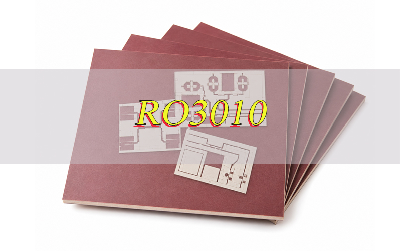
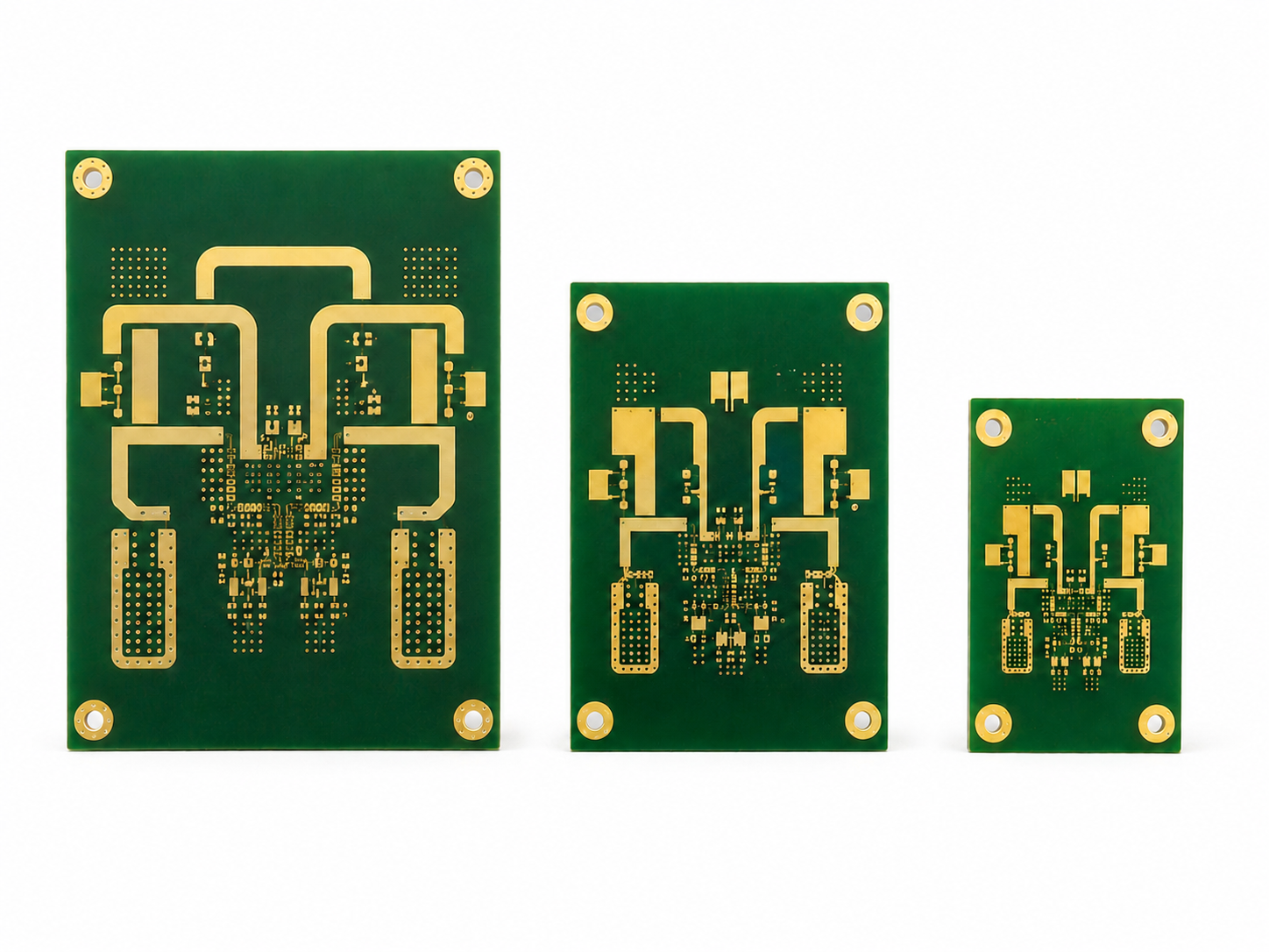
Rogers 3010 material usually refers to Rogers RO3010 laminate. It is a ceramic-filled PTFE composite circuit material designed for high-frequency PCB work. The material belongs to the Rogers RO3000 series, which is widely used for RF and microwave circuits.
In simple terms, it is not standard FR4. FR4 works well for many general electronic boards, while this Rogers material is used when signal stability, dielectric control, and low loss matter more.
The high dielectric constant helps reduce circuit size. This is useful for compact antennas, filters, RF modules, and microwave layouts where board space is limited.
This laminate also has low moisture absorption and controlled thermal expansion. These properties help the PCB keep stable electrical behavior under heat, humidity, and production stress.
Why Choose Rogers RO3010 for High-Frequency PCB Design?
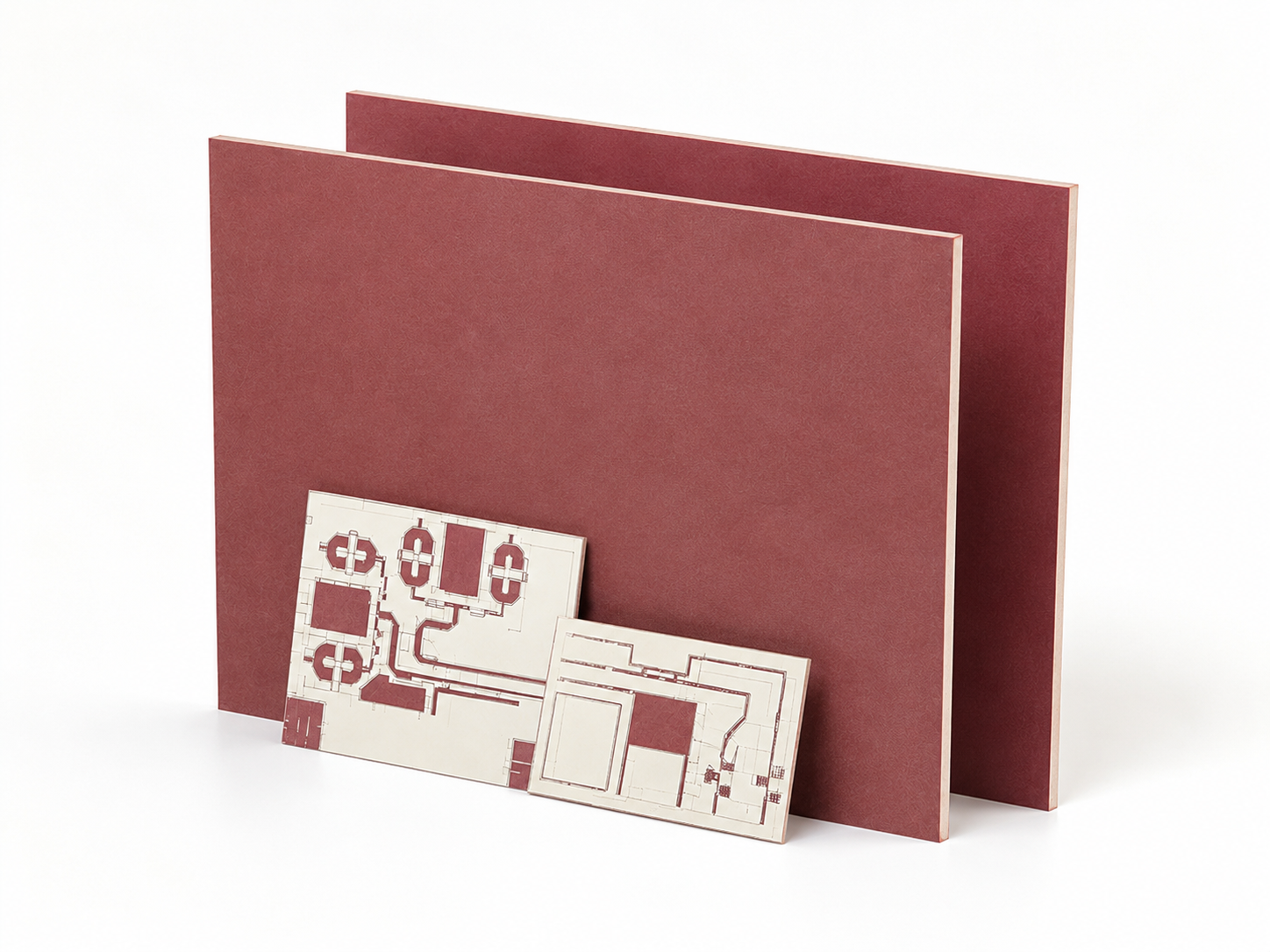
This material is chosen when a PCB needs compact RF layout, stable high-frequency behavior, and better signal control than standard FR4. Its high Dk allows shorter trace structures, while its low loss helps RF signals pass with less energy loss.
- High Dk: Supports smaller RF layouts and compact antenna structures.
- Low dissipation factor: Helps reduce signal loss at microwave frequency.
- Stable CTE: Helps the board remain stable during thermal stress.
- Good dimensional stability: Supports tighter line width and spacing control.
- Multilayer support: Can support multilayer PCB builds when the stackup is reviewed carefully.
- RF application fit: Suitable for RF modules, patch antennas, filters, and communication boards.
How Thick Is the RO3010?
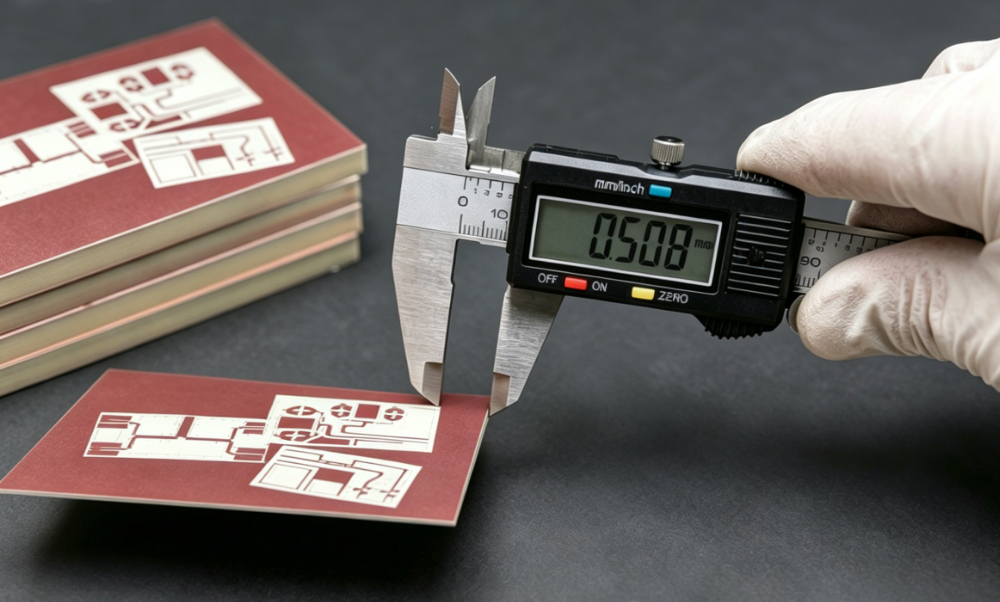
The standard laminate thicknesses of RO3010 include 0.005 in, 0.010 in, 0.025 in, and 0.050 in. These are about 0.13 mm, 0.25 mm, 0.64 mm, and 1.28 mm.
The correct thickness depends on the impedance target, copper weight, working frequency, RF trace width, and board stackup. A thinner substrate may suit some high-frequency layouts, while a thicker substrate may fit other impedance or mechanical needs.
Thickness should not be selected only from a catalog. In high-frequency work, even a small thickness change can affect impedance, phase, and antenna behavior.
For PCB fabrication, it is better to send Gerber files, stackup notes, impedance requirements, and copper weight together. This helps the manufacturer review material fit before production.
What Is the Dielectric Constant of RO3010?
RO3010 has a process Dk of 10.20 ± 0.30 at 10 GHz and a design Dk of 11.20. The process Dk helps explain material test data, while the design Dk is more useful for circuit calculation.
This high Dk is the main reason many RF layouts use this substrate. A higher Dk allows the same circuit function to fit into a smaller board area.
Dk also affects impedance, signal velocity, antenna size, and phase behavior. For this reason, the stackup and trace width should be reviewed before fabrication.
Do not treat Dk as a single number without context. Copper thickness, dielectric height, surface finish, etching control, and layout geometry can all change the final PCB result.
Rogers RO3010 Datasheet Overview
The RO3010 datasheet gives the basic material values needed for RF PCB design and fabrication review. And the relevant tables and PDF documents from the Rogers RO3010 datasheet are listed below for your reference.
| Item | Typical Value |
|---|---|
| Material type | Ceramic-filled PTFE composite |
| Process Dk | 10.20 ± 0.30 at 10 GHz |
| Design Dk | 11.20 |
| Dissipation factor | 0.0022 at 10 GHz |
| Thermal coefficient of Dk | -395 ppm/°C |
| Moisture absorption | 0.05% |
| Thermal conductivity | 0.95 W/m/K |
| X/Y/Z CTE | 13 / 11 / 16 ppm/°C |
| Copper peel strength | 9.4 lb/in |
| Density | 2.8 g/cm³ |
| Flammability rating | UL 94 V-0 |
| Lead-free process compatible | Yes |
These values are useful for material review, but final PCB performance still depends on stackup, etching control, lamination, drilling, plating, and inspection.
Rogers RO3010 vs RO3003 vs RO3006: What Is the Difference?
RO3003, RO3006, and RO3010 are ceramic-filled PTFE materials in the same series. The main difference is Dk. Lower Dk gives larger circuit size and often lower loss, while higher Dk supports more compact RF layout.
| Item | RO3003 | RO3006 | RO3010 |
|---|---|---|---|
| Material family | RO3000 series | RO3000 series | RO3000 series |
| Material type | Ceramic-filled PTFE composite | Ceramic-filled PTFE composite | Ceramic-filled PTFE composite |
| Process Dk | 3.00 ± 0.04 | 6.15 ± 0.15 | 10.20 ± 0.30 |
| Design Dk | 3.16 | 6.40 | 11.20 |
| Dissipation factor | 0.0010 at 10 GHz | 0.0020 at 10 GHz | 0.0022 at 10 GHz |
| Thermal coefficient of Dk | -3 ppm/°C | -262 ppm/°C | -395 ppm/°C |
| Water absorption | 0.04% | 0.02% | 0.05% |
| Thermal conductivity | 0.50 W/m/K | 0.79 W/m/K | 0.95 W/m/K |
| X/Y/Z CTE | 17 / 16 / 25 ppm/°C | 17 / 17 / 24 ppm/°C | 13 / 11 / 16 ppm/°C |
| Copper peel strength | 12.7 lb/in | 7.1 lb/in | 9.4 lb/in |
| Density | 2.1 g/cm³ | 2.6 g/cm³ | 2.8 g/cm³ |
| Flammability rating | UL 94 V-0 | UL 94 V-0 | UL 94 V-0 |
| Lead-free process compatible | Yes | Yes | Yes |
RO3003 is often used when low loss and wider RF structures are preferred. RO3006 sits in the middle. The high-Dk grade in this comparison is more suitable when small circuit size is a major goal.
What Design Factors Affect Rogers RO3010 PCB Performance?
Good material selection is only the first step. The final board result also depends on how the layout and fabrication rules are controlled.
- Dielectric thickness: It directly affects impedance and trace size.
- Copper weight: It changes trace height, etching behavior, and RF loss.
- Trace geometry: RF trace width, spacing, bends, and ground shape need careful control.
- Copper roughness: Rough copper can increase conductor loss at high frequency.
- Via structure: Via size, stub length, plating, and grounding vias affect RF return path.
- Stackup design: Hybrid builds with FR4 or other materials need thermal and mechanical review.
- Surface finish: ENIG, immersion silver, or other finishes should match RF needs and assembly flow.
- Fabrication tolerance: Line width, spacing, registration, drilling, and plating control all matter.
- Testing plan: Electrical test, impedance test, AOI, and visual inspection help confirm build quality.
What Applications Use Rogers RO3010 Substrate?
This substrate is used where high-frequency signals, compact layout, and material stability matter. It appears in antenna systems, communication systems, compact RF modules, and microwave boards.
- RF antenna PCB
- Patch antenna
- GPS antenna board
- Microwave circuit board
- RF filter board
- Satellite communication module
- Cellular communication antenna
- Broadband RF component
- Cable system datalink board
- Automotive radar-related RF board
- Wireless communication module
- High-frequency test board
For many of these uses, standard FR4 may not provide enough Dk stability or low-loss behavior at higher frequency. This high-Dk substrate gives a more suitable base for RF signal control.
How Much Does Rogers RO3010 PCB Material Cost?
The material cost is not a fixed number. The ro3010 price changes with laminate thickness, copper cladding, panel size, stock status, order quantity, and fabrication requirements.
The final PCB price also depends on board size, layer count, hole structure, impedance tolerance, surface finish, testing method, and delivery schedule. A simple 2-layer RF board and a multilayer RF board will not have the same cost level.
Material waste is another factor. If the board outline does not fit the panel size well, usable panel area may drop and cost can rise.
For a more accurate quote, prepare Gerber files, stackup, material thickness, copper weight, surface finish, quantity, and test requirements. These details allow a PCB manufacturer to calculate the cost more clearly.
How Can EBest Circuit Support Rogers RO3010 PCB Manufacturing?
EBest Circuit can support this type of RF PCB project from material review to production-quality fabrication. For RF boards, early technical review helps reduce impedance drift, layout risk, and manufacturing uncertainty before production begins.
- Material selection review for Rogers high-frequency laminates
- Stackup planning based on frequency, impedance, copper weight, and board thickness
- DFM review before fabrication to find spacing, via, copper, and panelization issues
- Controlled impedance fabrication for RF traces and transmission lines
- Rogers PCB fabrication for prototypes, small batches, and volume production
- Surface finish support such as ENIG, immersion silver, and other project-based finishes
- AOI, electrical test, visual inspection, and impedance test support
- Component sourcing and PCBA assembly for complete electronics manufacturing needs
- Production traceability for material batch, process flow, inspection, and shipment records
FAQs About Rogers RO3010 PCB Material
Q1: Is Rogers 3010 the same material as RO3010?
A1: Yes. Rogers 3010 usually refers to Rogers RO3010, a ceramic-filled PTFE high-frequency laminate in the RO3000 series. It is mainly used for RF, microwave, antenna, and compact high-frequency PCB designs.
Q2: Which Dk value should be used for RF circuit calculation?
A2: For design work, the more useful value is usually the design Dk of 11.20. The material also has a process Dk of 10.20 ± 0.30 at 10 GHz. In practical PCB fabrication, the final impedance result also depends on dielectric thickness, copper weight, trace width, and process tolerance.
Q3: What thicknesses are commonly available for this laminate?
A3: Common thicknesses include 0.005 in, 0.010 in, 0.025 in, and 0.050 in, which are about 0.13 mm, 0.25 mm, 0.64 mm, and 1.28 mm. The right thickness should match the target impedance, frequency, copper thickness, and stackup structure.
Q4: Why is this material often used for compact RF circuits?
A4: It has a high dielectric constant, so RF structures can be made smaller than many lower-Dk materials. Its design Dk of 11.20 helps reduce circuit size, which is useful for compact antennas, filters, microwave modules, and space-limited RF boards.
Q5: Can it be used for multilayer PCB fabrication?
A5: Yes. It can be used in multilayer PCB structures, but the stackup needs careful review. The manufacturer should check bonding material, lamination flow, drilling quality, copper plating, and impedance control before production.
Q6: Is it better than standard FR4?
A6: It depends on the application. For general electronic boards, FR4 is still practical and cost-friendly. For high-frequency circuits, this material provides better RF stability because it offers high Dk, low dissipation factor, and more stable high-frequency behavior than standard FR4.
Q7: What mainly affects PCB price for this material?
A7: The final price is affected by laminate thickness, copper weight, board size, layer count, impedance tolerance, surface finish, testing requirements, material availability, and lead time. A 2-layer RF board and a complex multilayer RF board will have very different costs.
Q8: What files should be prepared before requesting a quote?
A8: For a faster and more accurate quote, prepare Gerber files, stackup details, material thickness, copper weight, surface finish, quantity, impedance requirements, and test requirements. These details help the PCB manufacturer review manufacturability and calculate cost more accurately.
Q9: Can this laminate be combined with FR4 in a hybrid PCB stackup?
A9: Yes, hybrid stackups are possible. However, this laminate and FR4 have different material behavior, so the board needs review for thermal expansion, bonding reliability, drilling parameters, registration accuracy, and lamination control.
Q10: When should I choose this material instead of RO3003 or RO3006?
A10: Choose it when the design needs higher Dk and smaller RF circuit size. RO3003 is better for lower-Dk, low-loss RF layouts, while RO3006 sits between RO3003 and the high-Dk grade. This material is more suitable for compact RF antennas, filters, and microwave circuit boards.
Conclusion
Rogers RO3010 is a strong choice for high-frequency PCB projects that need high Dk, compact RF layout, stable signal transmission, and precise fabrication control. However, good material alone does not guarantee good board performance. The final result depends on thickness selection, copper weight, stackup design, impedance control, drilling quality, surface finish, and inspection process.
Ready to turn your Rogers RO3010 design into a reliable PCB? Send your Gerber files, stackup details, material thickness, copper weight, impedance requirements, quantity, and delivery needs to sales@bestpcbs.com. EBest Circuit can support your project with DFM review, material selection guidance, controlled impedance PCB fabrication, RF PCB manufacturing, testing, and production traceability. Get a clear quotation and practical manufacturing suggestions before your next build starts.
You may also like
Tags: ro3010 datasheet, ro3010 dielectric constant, ro3010 thickness, rogers ro3010, rogers ro3010 datasheet