

Heavy copper PCB is designed for applications that need higher current capacity, stronger thermal performance, and better mechanical reliability than standard circuit boards can offer. It is widely used in power electronics, industrial control, automotive systems, energy equipment, and other high-load environments.
At EBest Circuit, we manufacture heavy copper boards with stable process control, practical DFM support, and flexible build options for both prototype and production orders.
What Is a Heavy Copper PCB?
A heavy copper PCB is a printed circuit board built with much thicker copper conductors than a conventional PCB. In the PCB industry, the term usually refers to boards with 3 oz/ft² to 10 oz/ft² copper on the inner layers, outer layers, or both. For more demanding power applications, extreme heavy copper PCB can reach 20 oz/ft² to 200 oz/ft².
These boards are built to handle:
- Higher current loads
- Better heat transfer
- Improved resistance to thermal stress
- Longer service life in harsh operating conditions
Compared with standard copper boards, heavy copper PCBs are better suited for power conversion, current distribution, and heat-intensive designs.
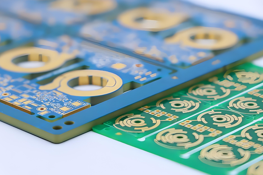
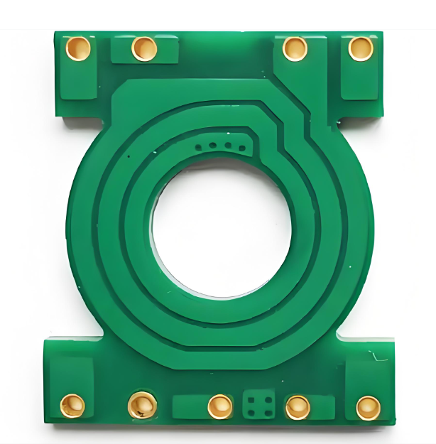
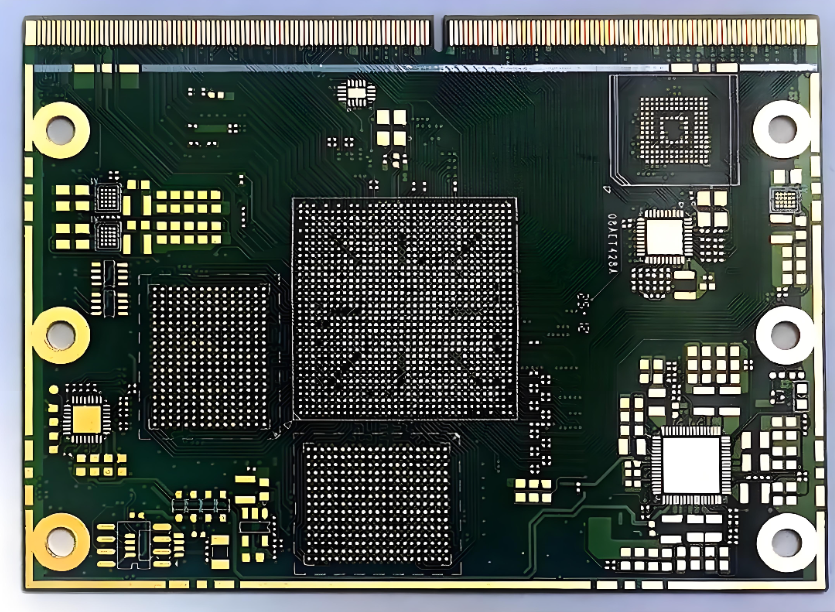
Heavy Copper PCB
Why Choose Heavy Copper PCB?
When a design involves high current, high power density, or repeated thermal cycling, standard copper thickness may no longer be enough. Heavy copper PCB provides a more reliable platform for these conditions. Below are the key benefits of using heavy copper PCB:
Higher Current Carrying Capacity
Thicker copper traces can carry more current safely and reduce the risk of overheating.
Better Thermal Management
Heavy copper helps spread and transfer heat more effectively, which supports stable performance in power circuits.
Improved Mechanical Strength
The copper structure adds durability and helps the board withstand demanding operating environments.
Better Reliability in Harsh Conditions
Heavy copper boards perform well in applications exposed to vibration, thermal shock, and continuous electrical load.
Fewer Design Limits for Power Routing
For power electronics, thicker copper offers more flexibility when routing high-current paths.
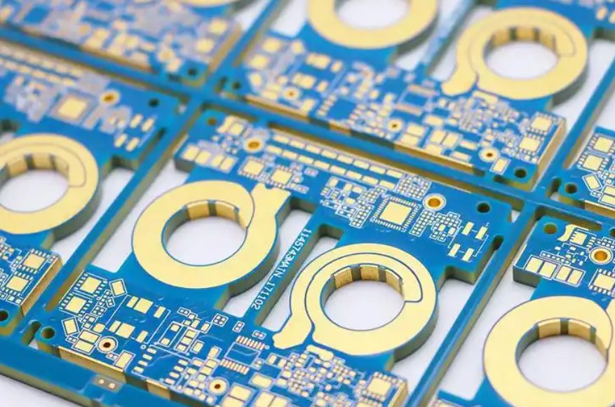
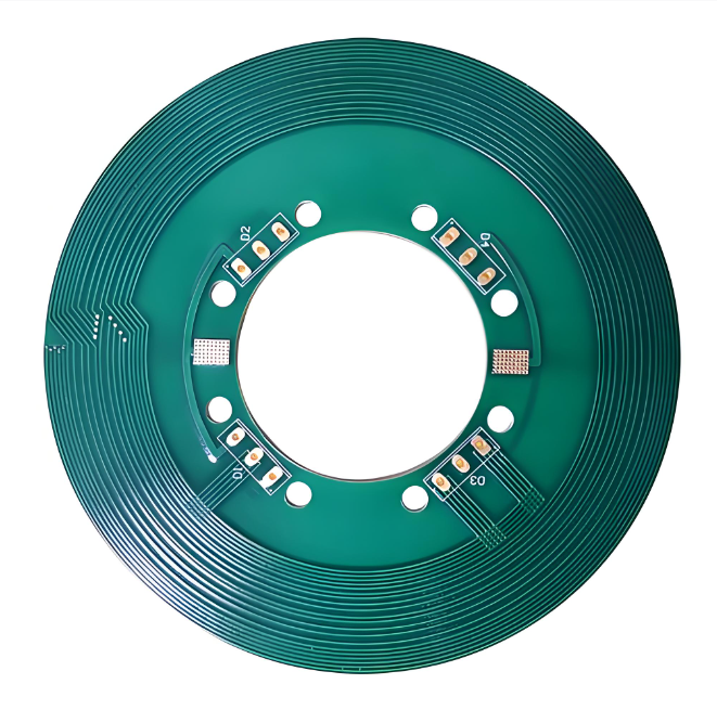
Heavy Copper PCB

Typical Applications of Heavy Copper PCB
Heavy copper PCBs are widely used in products where electrical load and heat generation are significant.
Common Applications Include:
- Power distribution systems
- Power converters
- Planar transformers
- Industrial control equipment
- Motor drives
- Automotive power electronics
- Solar and renewable energy systems
- Battery charging and energy storage equipment
- Welding equipment
- Heat dissipation modules
If your project needs stable current flow and efficient heat handling, heavy copper PCB is often the more suitable choice.
Heavy Copper PCB Design Considerations
Heavy copper board design is different from standard PCB design. Thicker copper affects current capacity, thermal behavior, trace geometry, and manufacturability. A good design should balance electrical performance with production feasibility.
1. Current Carrying Requirements
The minimum conductor width and copper thickness should be based on:
- Required current
- Acceptable temperature rise
- Board layout space
- Heat dissipation conditions
Wider traces and thicker copper improve current handling, but they also affect routing density and process difficulty.
2. Copper Profile and Manufacturing Impact
Heavy copper traces may not form a perfect rectangular shape after fabrication. The final conductor profile depends on plating and etching methods. This should be considered in spacing and tolerance planning.
3. Board Thickness
Heavy copper layers can increase total PCB thickness. This may affect:
- Mechanical assembly
- Connector matching
- Drilling process
- Stack-up design
- Final product dimensions
4. Preferred Fabrication Method
For many heavy copper boards, additive plating processes are preferred over subtractive etching. Additive processing offers better copper build-up control, though it usually increases fabrication cost.
5. Tolerance
Typical tolerance for conductor width, spacing, and thickness is around ±20%, although tighter control may be achievable depending on the board structure and manufacturing process.
Pls visit heavy copper PCB design guide for more information about design guide, or visit heavy copper PCB FAQ to make your heavy copper PCB design meet DFM better.
Our Heavy Copper PCB Capabilities
We support heavy copper PCB manufacturing for a wide range of power and thermal applications.
| Item | Capability |
| Base Material | FR4 / Aluminum |
| Copper Thickness | 4 oz to 10 oz |
| Extreme Heavy Copper | 20 oz to 200 oz |
| Board Outline | Routing, Punching, V-Cut |
| Solder Mask Color | White, Black, Blue, Green, Red |
| Surface Finish | Immersion Gold, HASL, OSP |
| Max Panel Size | 580 × 480 mm (22.8″ × 18.9″) |
If your project has special stack-up, thermal, or current requirements, we can review the design and suggest a more manufacturable solution.
How We Support Heavy Copper PCB Projects?
For heavy copper PCB, engineering review is often as important as manufacturing itself. We work with customers on the practical points that affect both performance and yield.
Our support can include:
- Copper thickness selection
- Trace width and spacing review
- Stack-up recommendation
- Thermal structure assessment
- Panelization suggestion
- DFM optimization before production
- Process evaluation for extreme heavy copper requirements
Heavy Copper PCB FAQ
1. What copper thickness is considered heavy copper PCB?
In general, heavy copper PCB refers to boards with copper thickness from 3 oz to 10 oz on inner or outer layers. Boards above this range, such as 20 oz to 200 oz, are often called extreme heavy copper PCB.
2. What is the main advantage of heavy copper PCB?
The main advantage is the ability to handle higher current and better heat dissipation compared with standard copper PCBs.
3. Can heavy copper PCB use aluminum base material?
Yes. Heavy copper PCB can be built on FR4 or aluminum base material, depending on the thermal and structural needs of the application.
4. Is heavy copper PCB more difficult to manufacture?
Yes. Thicker copper increases the complexity of plating, etching, drilling, and tolerance control. That is why DFM review is important before production.
5. What industries use heavy copper PCB most often?
Heavy copper PCB is commonly used in industrial control, automotive electronics, renewable energy, power conversion, and power distribution systems.
Request a Quote for Heavy Copper PCB
Looking for a reliable heavy copper PCB manufacturer?
EBest Circuit supports your project from design review to mass production with engineering-driven solutions and stable manufacturing capability.
Send us your Gerber files, stack-up, and technical requirements today.
📧 Email: sales@bestpcbs.com
📞 Tel: +86-755-2909-1601
You may also like
Tags: embedded copper pcb, heavy copper pcb, heavy copper pcb design, Heavy copper PCB manufacturer