

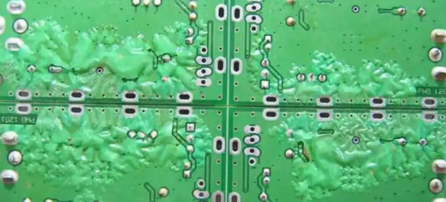
If you design or manufacture high-power electronics—such as LED modules, automotive electronics, or power supplies—you have likely encountered a costly issue: solder mask ink blistering or peeling on thermally conductive, copper-based PCBs.
This defect is far more than cosmetic. Once the ink detaches, insulation is compromised, copper is exposed, and the risk of corrosion, short circuits, and field failures increases sharply. The question is not if it can happen, but why it happens so often on thermally conductive PCBs—and how to prevent it in a controlled, repeatable way.
This guide explains the real root causes and provides a practical, engineering-driven prevention strategy.
Why Do Thermally Conductive PCBs Suffer from Ink Blistering?
Thermally conductive PCBs are designed to dissipate heat efficiently, often using thick copper layers, metal cores, or high-performance dielectric materials. These features make them excellent thermal performers—but also introduce mechanical stress.
The core issue is CTE mismatch. Copper, dielectric layers, substrates, and solder mask ink all expand and contract at different rates when exposed to heat. During soldering and thermal cycling, this mismatch generates strong shear forces at the ink-to-copper interface.
When stress exceeds adhesion strength, failure occurs. The ink does not fail randomly—the bond fails at its weakest point.
What Actually Fails When Ink Blisters or Peels Off?
The final failure mode is always the same: loss of adhesion between the solder mask ink and the copper surface.
Once this bond weakens:
- Heat causes localized lifting
- Trapped moisture expands into vapor
- Flux chemicals penetrate the interface
- The ink blisters, cracks, or peels away
Understanding why adhesion weakens is the key to long-term prevention.
Why Does Ink Adhesion Fail on Thermally Conductive PCBs?
Ink adhesion failure is rarely caused by a single factor. In most cases, it is the result of multiple small weaknesses stacking together.
1. Poor Surface Preparation
This is the most common root cause. Any contamination—oxide layers, oils from handling, dust, or residual plating chemicals—prevents proper bonding. Even a surface that is too smooth can be a problem, as the ink has nothing to mechanically anchor to.
Moisture trapped in vias or micro-voids becomes steam during soldering, pushing the ink away from underneath.
2. Using the Wrong Type of Ink
Standard solder masks developed for FR-4 are not designed for metal-core or high-thermal-conductivity boards. Their mechanical flexibility and thermal resistance are insufficient for the stress environment.
Expired ink or ink stored outside recommended conditions further degrades adhesion performance.
3. Incomplete or Incorrect Curing
Ink that is not fully cured remains chemically weak. Fast ramp rates, uneven oven temperatures, or insufficient soak time prevent full polymer cross-linking.
Visually, the ink may look acceptable—but internally, it lacks structural strength.
4. Chemical Attack During Assembly
Highly active fluxes can migrate under poorly bonded ink edges. Under reflow temperatures, these chemicals aggressively attack the interface, triggering sudden blistering or peeling after assembly.
5. Design-Driven Thermal Stress
Large copper pours and thick copper planes act as stress concentrators. Repeated thermal cycling during soldering, testing, and operation gradually fatigues the ink bond in these high-stress zones.
How Can Surface Preparation Be Optimized for Ink Adhesion?
The goal of surface preparation is simple: clean, micro-roughened, and moisture-free copper.
Key actions include:
- Using controlled acidic cleaning followed by high-pressure DI water rinsing
- Applying chemical micro-etch or plasma treatment to achieve Ra 0.4–0.8 µm
- Enforcing a strict “print within 2 hours” window after surface treatment
- Avoiding manual handling after preparation
Surface preparation sets the foundation. If this step fails, no ink can compensate.
How Should Ink Be Selected and Handled for These Boards?
Ink selection must match the application environment.
Best practices include:
- Using solder mask inks specifically qualified for metal-core or high-thermal PCBs
- Reviewing technical data sheets and Certificates of Analysis
- Storing ink at controlled temperature and humidity
- Enforcing FIFO inventory and never using expired material
Ink should be treated as a critical chemical, not a consumable.
What Printing and Curing Controls Prevent Ink Failures?
Printing and curing are where most hidden failures originate.
To maintain consistency:
- Control ink viscosity using a viscometer
- Measure dried ink thickness regularly (typically 25–35 µm)
- Ensure uniform coverage across thick copper areas
- Profile curing ovens using actual board measurements
Curing must follow the ink supplier’s recommended ramp-and-soak profile exactly. Assumptions are not acceptable—verification is required.
How Can Ink Reliability Be Validated Before Shipment?
Validation should simulate real assembly and field conditions.
Recommended tests include:
- Cross-hatch tape adhesion testing (IPC-TM-650 2.4.28)
- 288°C solder float testing
- Multiple simulated reflow cycles
- Compatibility testing with selected solder pastes and fluxes
If ink survives these tests, it is far more likely to survive real use.
How Can PCB Design Reduce Ink Stress and Blistering Risk?
Design choices strongly influence ink reliability.
Effective DFM measures include:
- Using rounded corners on large copper pours
- Adding solder mask anchor features where possible
- Avoiding abrupt copper thickness transitions
- Communicating ink and assembly risks early in design reviews
Design collaboration prevents problems that manufacturing alone cannot fix.
Why Is Pre-Bake Important Before Assembly?
Moisture is a silent contributor to blistering.
Pre-baking boards at 125°C for 1–2 hours before assembly removes absorbed moisture from substrates and vias. This simple step dramatically reduces steam-induced ink lifting during reflow.
How Should Ink Blistering Be Troubleshot Systematically?
When failures occur, follow a structured approach:
- Observe the blistering pattern
- Large, uniform blistering usually points to curing or ink issues
- Localized blistering often indicates contamination or handling problems
- Failures only after soldering suggest incomplete cure or flux attack
Systematic analysis saves time and prevents repeated mistakes.
What Is the Key to Preventing Ink Blistering Long Term?
Ink blistering on thermally conductive PCBs is not random. It is the result of unmanaged stress and weak process control.
Prevention comes from:
- Proper material selection
- Controlled surface preparation
- Verified curing processes
- Design collaboration
- Assembly compatibility planning
When these elements are managed together, ink blistering becomes a rare exception rather than a recurring problem.
Ready to Eliminate Ink Blistering on Thermally Conductive PCBs?
Ink blistering and solder mask peeling are not inevitable problems—they are signals that something in material selection, process control, or design collaboration needs to be improved.
If you are working with thermally conductive, copper-based, or metal-core PCBs and want to prevent ink failures before they reach assembly or the field, working with an experienced manufacturing partner makes a measurable difference.
At EBest Circuit, we support engineers with:
- Early DFM and process risk review for thermally conductive PCBs
- Proven solder mask and surface treatment processes for high-thermal designs
- Full PCB + PCBA one-stop service, including testing and traceability
- Prototype and small-volume support with fast technical feedback
If you’d like a second opinion on your board design, process flow, or ink-related reliability risks, feel free to contact our engineering team.
📩 Email: sales@bestpcbs.com
We’re here to help you turn thermal performance into long-term reliability—without surprises after reflow.
Tags: copper based pcb, ink blistering on pcb, Metal Core PCB, pcb failures