

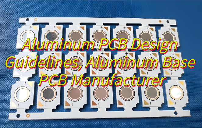
Looking for aluminum PCB design guidelines? Let’s discover design specifications, design tools, design guidelines for aluminum PCB, and how to get a quote through this blog.
Are you worried about these issues?
- LED lighting/power modules generate serious heat when running for a long time. How to ensure the stable heat dissipation performance of aluminum substrates?
- The procurement cost of aluminum substrates accounts for 15%-20% of the production cost. How to balance performance and price?
- Under complex wiring requirements, how to break through the limit of the number of layers of aluminum substrates to achieve high-density integration?
EBest Circuit (Best Technology) can provide:
- Gradient heat dissipation solution: customized 1.5-3.0W/m·K thermal conductivity plates; embedded copper pillar technology improves local heat dissipation efficiency by 30%.
- Supply chain cost optimization: direct procurement of 6000 series aviation aluminum materials, reducing costs by 12%; panel production mode reduces material waste by 18%.
- HDI aluminum-based stacking technology: supports 1-6 layers of arbitrary laminated structure; laser blind hole accuracy ±0.05mm.
Welcome to contact EBest Circuit (Best Technology) if you have any request for aluminum base PCB design, manufacturing or assembly: sales@bestpcbs.com.
What Is Aluminum PCB Design Guideline?
Aluminum PCB design guidelines defines the principles for creating circuit boards with a metal (typically aluminum) core, optimized for thermal management in high-power applications. It focuses on selecting thermally conductive dielectric layers, strategic component placement to leverage the aluminum base’s heat dissipation, and ensuring mechanical durability while balancing electrical performance and reliability in heat-intensive environments.
Aluminum PCB Design Specifications
| Parameter | Value/Range |
| Thermal Conductivity | 1.0–8.0 W/m·K (Material-dependent) |
| Copper Thickness | 1oz (35µm) to 10oz (350µm) |
| Dielectric Strength | ≥3000V (Standard), AC1500V–6000V (High-voltage) |
| Thermal Resistance | 1.0–2.5°C/W (Full PCB) |
| Max Operating Temperature | 150–260°C (Peak) |
| Peel Strength | ≥1.0 N/mm (Post-thermal stress) |
| CTE Mismatch | Aluminum (23–24 ppm/°C) vs. Copper (17 ppm/°C) |
| Min Trace Width/Spacing | 0.1mm (4mil) outer layer, 0.13mm (5mil) inner |
| Via Wall Copper Thickness | 20–25µm (Standard), 35µm (High-current) |
| Board Thickness | 1.0–3.0mm (Aluminum core) |
Aluminum PCB Design Tools & Software
1. Altium Designer – Advanced Layout & Thermal Analysis
- Thermal simulations to prevent overheating.
- High-current trace routing for power-heavy designs.
- 3D modeling for enclosures and heat sink integration.
2. Automated DRC (Design Rule Check) for manufacturing compliance
- Cadence Allegro – High-Speed & High-Power PCB Design.
- Signal integrity analysis for high-frequency applications.
- Power delivery network (PDN) optimization.
- Multi-layer stackup design for rigid-flex aluminum boards.
3. KiCad – Free & Open-Source for Prototyping
- No licensing fees for startups/SMEs.
- Built-in footprint libraries for common aluminum PCBs.
- Gerber file generation for seamless manufacturing.
4. SolidWorks – Mechanical Integration for Thermal Management
- Heat sink modeling for custom cooling solutions.
- Mounting hole placement for industrial applications.
- Stress analysis for vibration-resistant designs.
5. Ansys Icepak – Advanced Thermal Simulation
- Precision heat flow modeling for high-power LEDs/motors.
- Fan and vent placement optimization.
- Material selection guidance for thermal conductivity.
Aluminum PCB Design Guidelines
1. Thermal Viability First
- Calculate required thermal vias using: N = (P × Rth)/ΔT, where P = power (W), Rth = thermal resistance (°C/W), and ΔT = max allowable temp rise. Aim for ≥6 vias (0.5mm dia) under high-power devices.
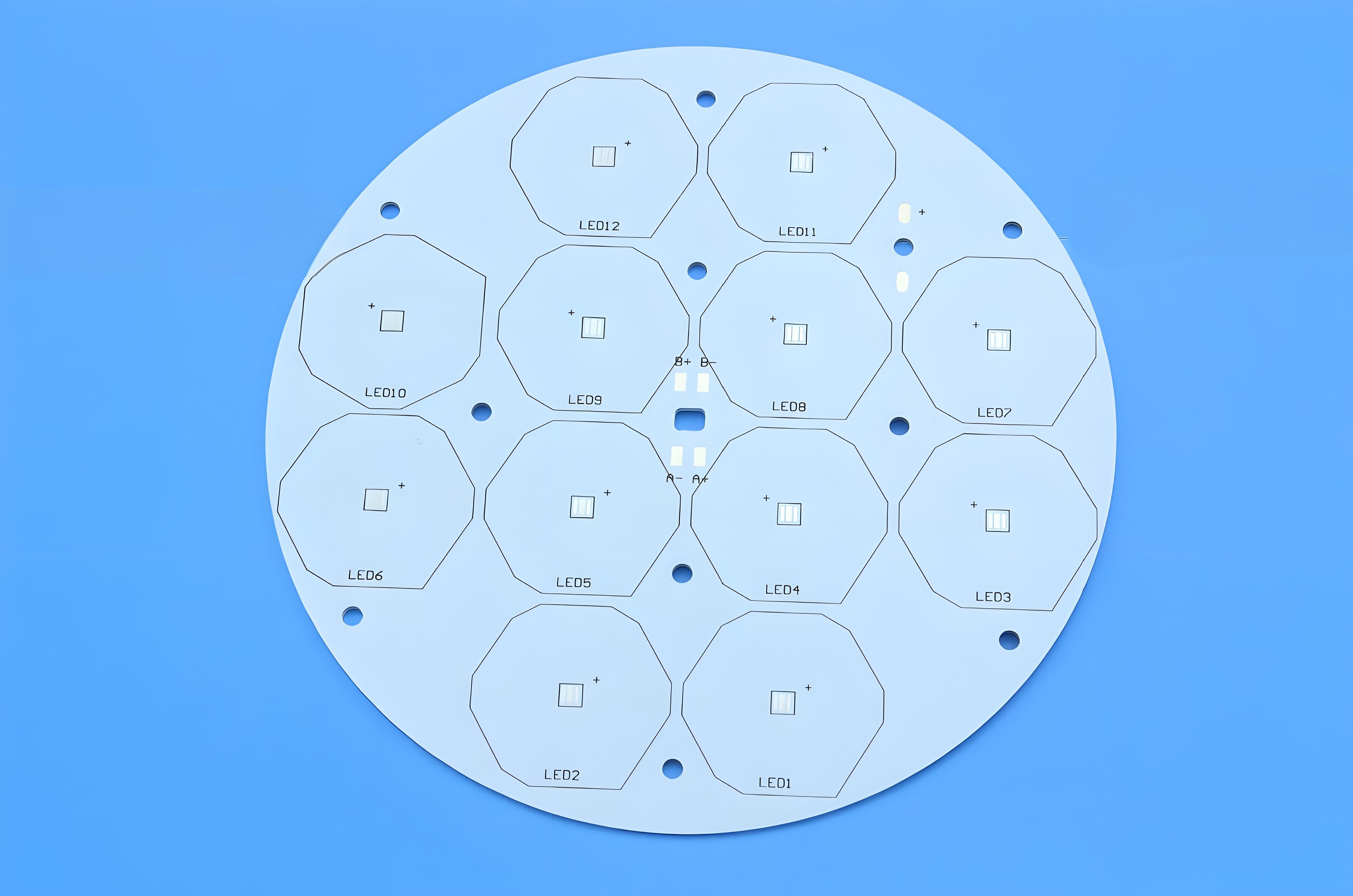
- For LEDs >1W, ensure die attach area covers ≥70% of the aluminum base. Use white solder mask to reflect unused light and reduce thermal load.
2. Component Placement Logic
- Group heat sources (e.g., regulators, drivers) in a central “thermal zone” with direct aluminum exposure. Keep analog/RF components ≥5mm from this zone to avoid thermal noise.
- Orient power transistors with drain/collector pads parallel to aluminum grain direction for optimal heat spreading.
3. Copper-Aluminum Bonding
- Use 35µm (1oz) copper for signals; switch to 70µm (2oz) for power traces. Avoid abrupt copper weight transitions (>1oz difference) to prevent lamination cracks.
- Specify “button plating” for plated through-holes (PTHs) to reinforce aluminum-copper joints.
- Dielectric Layer Control
- Request dielectric thickness tolerance of ±10%. Thinner layers (50µm) improve thermal performance but risk electrical breakdown; validate with V = E × d (E = dielectric strength, d = thickness).
- For high-voltage (>100V) designs, add a 50µm polyimide overlay on critical traces.
4. Mechanical Stress Mitigation
- Add 1mm chamfered edges to aluminum cores to prevent sharp corners causing board flex. Use 3M™ thermal tapes instead of screws for non-critical assemblies to reduce thermal impedance.
- For assemblies with >5kg weight, specify aluminum thickness ≥2.0mm and add 2mm mounting holes spaced ≥50mm apart.
5. Assembly Compatibility
- Require wave soldering temps ≤260°C for aluminum PCBs. Use low-melting-point solder (Sn42/Bi58) for mixed-technology boards (SMT + through-hole).
- Add 0.2mm solder mask dams between fine-pitch SMT pads to prevent solder wicking on aluminum surfaces.
6. Testing Protocols
- Perform IR thermal imaging at 80% max load for 2 hours. Target ΔT <15°C between hottest component and ambient. Validate dielectric integrity with 500V Hipot testing; fail if leakage current >5mA.
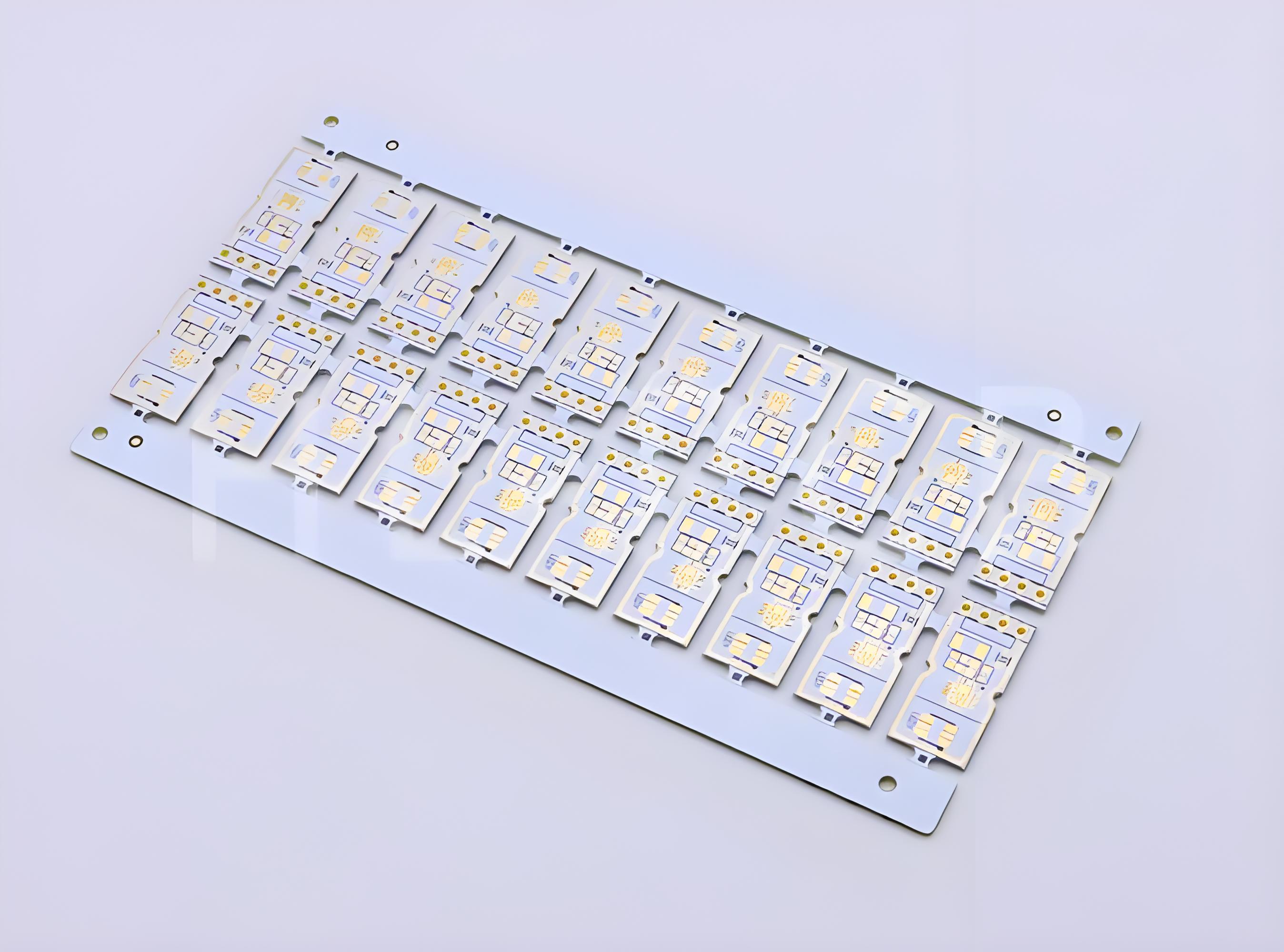
Aluminum Base PCB Manufacturing Processes
Below are aluminum base PCB manufacturing processes:
1. Material Preparation
- Aluminum Base Selection: Choose alloy (e.g., 5052, 6061) based on thermal/mechanical needs. Thickness ranges 1.0–3.0mm.
- Surface Treatment: Clean and roughen aluminum via chemical etching to improve dielectric adhesion.
2. Lamination
- Dielectric Layer Application: Coat aluminum with thermally conductive epoxy (1–8 W/m·K) or ceramic-filled prepreg.
- Copper Foil Bonding: Press 1–10oz copper foil onto the dielectric under 180–200°C and 15–20 kg/cm² pressure.
3. Circuit Imaging
- Dry Film Application: Laminate photosensitive dry film onto copper. Expose to UV light through a circuit mask.
- Etching: Use alkaline solution (e.g., sodium hydroxide) to remove unexposed copper, leaving precise traces.
4. Via Formation
- Mechanical Drilling: Drill microvias (0.2–0.5mm) using carbide bits. Deburr holes to remove aluminum shavings.
- Plating: Electroplate holes with 20–35µm copper to ensure conductivity and thermal transfer.
5. Solder Mask Application
- Screen Printing: Apply epoxy-based solder mask (white/black) to protect traces. Cure at 150°C for 60 minutes.
- Secondary Coating: Add high-temperature polyimide tape on power traces for >200°C environments.
6. Surface Finish
- HASL (Hot Air Solder Leveling): Dip PCB in molten solder (Sn63/Pb37) for cost-effective finish.
- ENIG (Electroless Nickel Immersion Gold): Apply 3–5µm nickel and 0.05–0.1µm gold for fine-pitch SMT.
7. Profiling & Testing
- Routing: Cut boards to shape using CNC machines. Add chamfered edges to prevent assembly damage.
- Electrical Testing: Use flying probe or bed-of-nails to verify continuity (≤1Ω) and isolation (≥100MΩ).
- Thermal Cycling: Expose PCB to -40°C/125°C cycles (5x) to validate reliability.
Why Choose EBest Circuit (Best Technology) as Aluminum Base PCB Manufacturer?
Reasons why choose EBest Circuit (Best Technology) as aluminum base PCB manufacturer:
Accelerated Time-to-Market
- 24-Hour Prototyping: Rapid sample delivery cuts initial validation time by 50%.
- 19-Year Production Expertise: Optimized workflows reduce lead times by 30% through proven scheduling and risk mitigation.
Cost Efficiency
- 15–20% Price Advantage: In-house aluminum processing and bulk material sourcing eliminate middleman markups.
- Transparent Pricing: No hidden fees for tooling, testing, or design revisions.
Reliable Quality
- Rigorous Testing: Every PCB undergoes thermal shock (-40°C to 125°C), vibration, and 100% electrical checks.
- Material Traceability: Lot-specific records ensure accountability for aluminum origin, plating batches, and test data.
Design Optimization
- Free DFM Review: Engineers adjust trace widths/vias to balance thermal performance and manufacturability.
- Thermal Simulation: ANSYS models predict heat flow, avoiding costly post-design fixes.
End to End Service
- Full Turnkey Solution: Integrate raw material sourcing, production, and testing under one roof, reducing client coordination effort.
- Stable Material Supply: Long-term partnerships with aluminum/copper suppliers prevent delays from shortages.
- 24/7 Emergency Support: Rapid response to design changes or urgent orders, minimizing downtime.
Our Aluminum Base PCB Manufacturing Capabilities
| Base material: | Aluminum Alloy |
| Thermal Conductivity (dielectric layer): | 0.8, 1.0, 1.5, 2.0, 3.0 W/m.K. |
| Board Thickness: | 0.5mm~3.0mm(0.02″~0.12″) |
| Copper thickness: | 0.5 OZ, 1.0 OZ, 2.0 OZ, 3.0 OZ, up to 10 OZ |
| Outline: | Routing, punching, V-Cut |
| Soldermask: | White/Black/Blue/Green/Red Oil |
| Legend/Silkscreen Color: | Black/White |
| Surface finishing: | Immersion Gold, HASL, OSP |
| Max Panel size: | 600*500mm (23.62″*19.68″) |
| Packing: | Vacuum/Plastic bag |
| Samples L/T: | 4~6 Days |
| MP L/T: | 5~7 Days |
Our Quality Inspection & Certification
- Certified & Compliant Standards: ISO 9001, ISO 13485, IATF 16949 Certified, and UL, REACH, RoHS Compliant
- AOI (Automated Optical Inspection): Detects surface defects like open/short circuits, missing components, and soldering issues.
- X-Ray Inspection (Internal Defect Screening): Checks solder joint voids, cracks, and BGA/QFN hidden defects.
- Aging Test: Includes thermal cycling (-40℃~85℃) and humidity exposure to validate long-term reliability.
- Dimensional Verification: Measures thickness (±0.1mm), flatness, and hole alignment accuracy.
How to Get a Quote for Your Metal Core PCB Project?
To get a quote for your metal core PCB project, submit the following materials:
- Gerber Files & Drill Data: Essential for manufacturing accuracy.
- Bill of Materials (BOM): Lists all components and their specifications.
- Technical Specs: Layer count, base material (e.g., aluminum/copper), copper thickness, board thickness, min. trace width/spacing, and impedance control requirements.
- Surface Finish: Specify HASL, ENIG, OSP, or other finishes.
- Special Requirements: Thick copper design, blind/buried vias, or thermal management needs.
- Quantity & Delivery Timeline: Project volume and urgency.
Contact EBest Circuit (Best Technology) today to get a free DFM analysis report: sales@bestpcbs.com.