

Multilayer PCB design is at the heart of compact, high-speed electronics. As more devices require higher functionality in smaller packages, multilayer PCBs have become the go-to solution. In this blog, we’ll explore how these boards are designed, what materials go into them, and how they are manufactured.
EBest Circuit (Best Technology) is a trusted PCB manufacturer based in China, specializing in small to medium-volume PCB fabrication, PCB assembly, and comprehensive electronic manufacturing services (EMS). As a one-stop PCB solutions provider, we go beyond manufacturing. Our services cover turnkey assembly, component sourcing, box build assembly, PCBA testing, and full electronics assembly. Whether you’re developing a prototype or scaling up to full production, EBest Circuit (Best Technology) is committed to delivering reliable quality, fast turnaround, and personalized support to meet all your PCB and electronics manufacturing needs.
What Is PCB Multilayer?
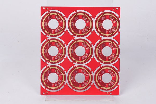
A multilayer PCB is a type of printed circuit board made by stacking multiple copper layers with insulating materials in between. While a single-sided PCB has only one conductive layer and a double-sided PCB has two, a multilayer PCB typically starts at four layers and can exceed thirty layers depending on the design complexity.
These copper layers are interconnected using vias (small plated holes). The main advantage is that multilayer PCBs allow more complex circuitry in a compact form. They’re used when simple routing becomes impossible due to high component density, high-speed signals, or design restrictions.
Multilayer boards usually contain signal layers, power planes, and ground planes that are symmetrically arranged to ensure electrical balance and mechanical stability.
Advantages of Multilayer PCB
There are many advantages of multilayer PCBs, especially for high-end, compact, and performance-driven applications:
- High Circuit Density: Multilayer PCBs offer more real estate by using multiple layers. This helps route more connections without crowding.
- Compact Size: By stacking layers, complex circuits can be condensed into smaller board sizes, which is important for modern gadgets.
- Better Signal Integrity: Ground and power planes shield signal layers, helping reduce electromagnetic interference and signal loss.
- Enhanced Reliability: Since many connections are internal and automated, multilayer PCBs tend to be more reliable than manually wired boards.
- Improved Power Distribution: Dedicated power planes help distribute power evenly across the board.
- Cost Efficiency in Mass Production: Although more expensive to design, they become cost-effective when produced at scale.
What Materials Are Used for Multilayer PCB?
Multilayer PCB construction involves several materials chosen based on the application’s electrical, thermal, and mechanical requirements. Common materials include:
- Copper Foil: Used for all conductive layers. Thickness ranges from 0.5oz to 3oz, depending on current requirements.
- Core Material (FR4): The most widely used substrate, made from fiberglass-reinforced epoxy. It provides mechanical strength and insulation.
- Prepreg (Pre-impregnated resin): A resin-impregnated fiberglass that bonds layers together during lamination.
- High-Frequency Materials: For applications like 5G or RF circuits, materials such as PTFE, Rogers, or ceramic substrates are used.
- Solder Mask: This green or colored coating protects the board from oxidation and solder bridges.
- Silkscreen: Printed on the board to mark component positions and labels.
For high-temperature or high-reliability applications, alternative materials like polyimide or metal cores may also be used.
Why Are There No 3 Layer PCBs?
Technically, you can make a 3-layer PCB, but they are very uncommon and often impractical. PCB manufacturing is designed to favor even-numbered layer configurations for several reasons:
1. Symmetry: Even-layered stack-ups offer better mechanical balance. Odd layers may lead to board warping due to uneven internal stress.
2. Manufacturing Simplicity: Most production lines are optimized for 4, 6, or 8 layers. A 3-layer board would require a custom process, which increases cost.
3. Signal Performance: High-speed signals benefit from a symmetrical structure. Odd-layer designs make it harder to maintain signal and power integrity.
Because of these reasons, designers usually move to 4-layer designs when they outgrow double-sided layouts.
How to Design a Multilayer PCB?
Designing a multilayer PCB starts with understanding the functional needs of your product. Here’s a step-by-step process:
- Define Layer Count: Decide how many layers are required based on circuit complexity, signal integrity, and available space. Common configurations include 4, 6, and 8 layers.
- Create a Stack-Up: Plan how each layer will function — signal, ground, or power. Layer arrangement impacts EMI performance and routing efficiency.
- Component Placement: Place high-speed, sensitive, and power components with care. Keep analog and digital sections separate.
- Routing Strategy: Route critical signals on inner layers to shield them from external noise. Use short, direct routes for clock and high-speed lines.
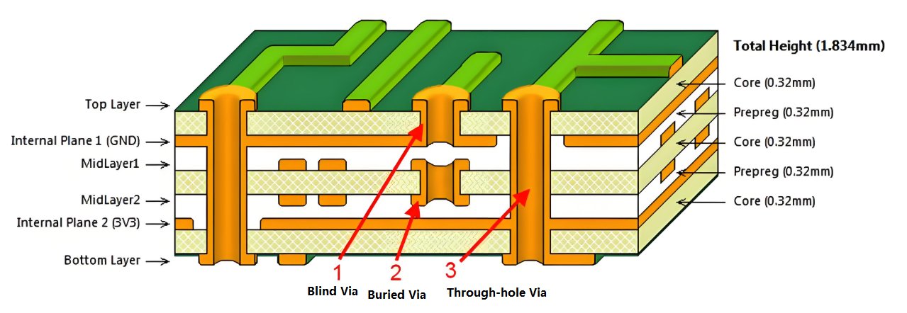
- Via Planning: Use through-hole vias, blind vias, and buried vias to connect different layers.
- Impedance Control: For high-speed signals, calculate and control the trace impedance using PCB design software.
- Thermal Management: Add thermal vias and consider copper pour for better heat distribution.
- Design for Manufacturability (DFM): Ensure trace widths, spacing, hole sizes, and clearances follow manufacturer guidelines.
Design tools like Altium Designer, Eagle, or KiCad can help streamline multilayer PCB design while checking for errors along the way.
How to Build a Multilayer PCB Stack-Up?
A stack-up is the arrangement of copper and dielectric layers in a multilayer PCB. It affects signal quality, EMI, thermal behavior, and mechanical strength.
Common 4-Layer Stack-Up:
- Top layer: Signal
- Inner layer 1: Ground
- Inner layer 2: Power
- Bottom layer: Signal
6-Layer Stack-Up Example:
- Top: Signal
- Layer 2: Ground
- Layer 3: Signal
- Layer 4: Signal
- Layer 5: Power
- Bottom: Signal
Tips for Effective Stack-Up:
- Keep ground and power layers close for decoupling.
- Place critical signals between ground planes.
- Symmetry reduces warping.
- Maintain consistent dielectric thickness to control impedance.
At EBest Circuit (Best Technology), our engineering team assists clients with stack-up planning to match their performance, size, and cost targets.
Multilayer PCB Manufacturing Process
The multilayer PCB manufacturing process involves combining multiple copper and insulation layers through precise steps:
1. Inner Layer Imaging
Each internal copper layer is printed with the desired circuit pattern using photoresist and UV light.
2. Etching
Unwanted copper is chemically etched away, leaving only the circuit traces.
3. Lamination
All layers are stacked with prepreg between them and laminated under high heat and pressure to form a single board.
4. Drilling
Holes are drilled through the stack to connect layers. These include through-hole, blind, and buried vias.
5. Plating
Copper is plated into drilled holes and on the board’s surface to create electrical paths.
6. Outer Layer Imaging and Etching
Outer layers undergo the same photoimaging and etching process as inner layers.
7. Solder Mask and Silkscreen Application
A solder mask is added to prevent oxidation and short circuits. Silkscreen is printed for component labeling.
8. Surface Finishing
Finishes like HASL, ENIG, or OSP are applied to pads for better solderability.
9. Testing and Inspection
Every board undergoes electrical tests and visual inspections to catch defects.
At EBest Circuit (Best Technology), we combine automated optical inspection (AOI), flying probe testing, and impedance measurement tools to ensure product quality at every stage.
Multilayer PCB Application
Multilayer PCBs are used in products where performance and miniaturization are critical. Here are some typical multilayer PCB applications:
- Smartphones and Tablets: Compact devices need high-density PCBs to fit advanced features in tight spaces.
- Medical Equipment: Imaging machines, heart monitors, and portable diagnostic tools depend on stable multilayer circuits.
- Automotive Electronics: Modern vehicles use multilayer PCBs for infotainment systems, sensors, and control units.
- Telecommunication Devices: Routers, switches, and 5G antennas rely on multilayer designs for signal integrity.
- Industrial Controls: Multilayer PCBs support automation equipment and high-voltage circuits.
- Military and Aerospace: Satellites, drones, and radar systems require rugged multilayer boards with excellent thermal and electrical performance.
How to Identify Multilayer PCB?
Identifying a multilayer PCB can be tricky just by looking at the surface. However, here are some tips:
- Edge View: Under a magnifier, you can often see multiple stacked layers at the board edge.
- X-ray Inspection: In factories, X-ray equipment can show internal connections and vias not visible from outside.
- Blind/Buried Vias: If the board has vias that don’t go through the entire thickness, it’s likely multilayer.
- Complexity and Component Density: A compact board handling many components usually suggests a multilayer design.
FAQs
1. What is the typical number of layers in a multilayer PCB?
Most commonly, multilayer PCBs have 4, 6, or 8 layers. High-end designs may go up to 32 or more.
2. Can multilayer PCBs be flexible?
Yes. Flexible multilayer PCBs are used in wearables, cameras, and aerospace applications where bending is needed.
3. Are multilayer PCBs expensive?
They cost more than single or double-layer PCBs but offer more value in space savings and performance.
4. What’s the difference between blind and buried vias?
Blind vias connect outer and inner layers. Buried vias connect internal layers only, and are hidden from the surface.
5. How does EBest Circuit (Best Technology) support multilayer PCB projects?
We offer complete support — design review, stack-up suggestions, high-speed materials, and full traceability via MES systems.
Tags: Advantages of multilayer pcb, multilayer pcb manufacturing process