Looking for cutting-edge robotics PCB design solutions that ensure precision and durability for your robotic applications? This guide covers everything from technical specifications to manufacturer selection for reliable robotic PCB production.
Best Technology stands out as a leading robotics PCB design manufacturer by combining engineering expertise with customer-centric services. Our advantage lies in offering free DFM (Design for Manufacturability) analysis – our engineers proactively identify potential production issues in your robotic PCB designs before fabrication, saving 15-30% revision time. With 5 dedicated high-mix PCB lines, we achieve 7-12 days standard lead times (30% faster than industry averages) for rigid-flex boards up to 20 layers, critical for agile robotics prototyping. Advanced capabilities include 6μm laser drilling for high-density interconnects in robotic joints and impedance control ±7% for motor control signals. We serve 40+ robotics clients globally with 98.2% on-time delivery and IPC Class 3 compliance for industrial-grade reliability. Contact us to experience how our free DFM + fast-turn service accelerates your robotics innovation cycle: sales@bestpcbs.com.
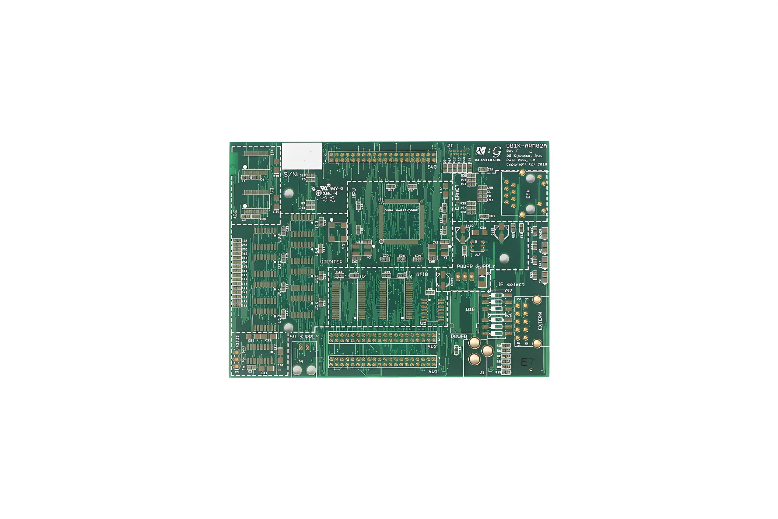
What Is Robotics PCB Design?
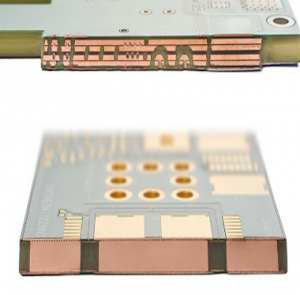
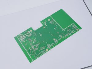
Robotics PCB design refers to the specialized process of creating printed circuit boards tailored for robotic systems. This discipline integrates electronic circuit layout with mechanical constraints unique to robotics, considering factors like dynamic motion tolerance, vibration resistance, and compact spatial requirements. Unlike conventional PCB design, robotics PCB design demands careful coordination between sensor interfaces, motor drivers, and onboard processors while accommodating three-dimensional movement patterns. The design must ensure reliable power distribution across articulated joints and maintain signal integrity despite electromagnetic interference from actuators. Successful implementations balance electrical performance with physical robustness, enabling autonomous navigation, precise manipulation, and real-time data processing within the robot’s operational environment. Modern approaches increasingly incorporate flexible circuits and modular architectures to support adaptive robotic behaviors.
What Are Features of Robotics PCB Design?
Here are features of robotics PCB design:
- Motion-Aware Layout – Circuit traces and components are arranged accounting for continuous mechanical movement, preventing stress fractures in solder joints during robotic arm articulation.
- Multi-Sensor Integration – Dedicated interfaces for LiDAR, IMU, and force/torque sensors maintain signal purity despite electromagnetic noise from nearby motors.
- Power Resilience – High-current paths for servo drivers incorporate thick copper pours (≥2oz) and redundant vias to handle sudden torque demands.
- Compact Stack-ups – Multilayer boards (6-12 layers) achieve high-density routing in confined spaces like robotic joints, using microvias for escape routing.
- Vibration Resistance – Components under 10g are secured with corner glue dots or underfill, while connectors use locking mechanisms.
- Real-Time Processing – FPGAs and MCUs are positioned to minimize latency in control loops, with careful clock distribution to avoid jitter.
- Environmental Hardening – Conformal coatings protect against dust/moisture, and thermal vias manage heat in sealed robotic enclosures.
- Modularity – Board-to-board connectors allow easy expansion, such as adding new gripper modules without redesigning the main controller.
- EMI Mitigation – Motor driver sections are isolated with moats and shielded with grounded copper fences to prevent interference with sensitive analog circuits.
- Field-Repairable Design – Critical components use socketed mounting or labeled test points for quick maintenance during robotic deployments.
Robotics PCB Design Technical Parameters
Technical parameters for robotics PCB design:
Dimensional and Layer Configuration
- Form Factor: Compact designs (e.g., 60mm×40mm to 200mm×150mm) to fit within robotic chassis, with mounting holes and mechanical interfaces pre-integrated.
- Layer Count: 4–16 layers depending on complexity, with dedicated power/ground planes for high-speed signals and isolation between analog/digital domains.
Material Selection for Robustness
- Substrate: High-Tg laminates (e.g., FR-408HR, Tg ≥ 170°C) to withstand thermal cycling in motor-driven or high-power applications.
- Flexible PCBs: Polyimide (PI) materials for dynamic bending applications (e.g., robotic arms), with laser-etched traces and reinforced stiffeners at critical stress points.
Electrical Performance
- Signal Integrity: Controlled impedance (50Ω ± 10%) for high-speed interfaces (e.g., CAN FD, EtherCAT), with differential pair length matching ≤2mil.
- Power Delivery: 2oz copper thickness for 24V motor driver traces, with via diameters ≥0.5mm to minimize voltage drop.
- EMC Compliance: Ring-shaped ground planes around noisy components (motors, wireless modules), spaced ≥0.5mm from signal traces.
Thermal Management
- High-Power Components: Copper pour areas ≥200mm² under MOSFETs/DC-DC converters, with thermal vias (≥8 per component, 0.3mm diameter) for heat dissipation.
- Simulation: Thermal mapping across -20°C to 85°C operating range, ensuring ≤30°C temperature rise for critical sensors.
Mechanical Reliability
- Vibration Resistance: Random vibration testing (5–2000Hz, 5Grms) with teardrop-shaped SMT pads to mitigate crack propagation.
- Shock Protection: “Crosshair” connector reinforcement for 50G impact resistance, preventing solder joint failure in mobile robots.
Connectivity and Expandability
- ESD Protection: TVS diodes for RJ45/USB-C ports, withstanding ≥±8kV surge events.
- Modular Interfaces: Gold-plated (≥3μin) expansion headers (e.g., Pmod, Arduino Shield) rated for ≥1000 mating cycles.
Design for Manufacturing (DFM)
- Trace/Space: Minimum 3mil line width/spacing for SMT compatibility, with solder mask dams between pads.
- Test Points: Dedicated vias for all power/ground/signal nets, spaced ≥1.27mm apart for flying probe testing.
Safety and Compliance
- Standards: IEC 60204-1 (machinery safety) and ISO 13849 (functional safety), with 1500V AC hipot testing for insulation.
- E-Stop Circuitry: Independent monitoring channel with ≤10ms response time to cut power during faults.
Advanced Trends
- Magnetic Current Sensors: Integrated solutions (e.g., Allegro ACS37041) for compact, high-accuracy current sensing in motor drives.
- AI-Driven Inspection: 3D AOI systems for detecting micro-defects (e.g., blind via filling, laser drilling residues) in HDI boards.
Design Consideration For Robotics PCB Design
Below are design consideration for robotics PCB design:
Component Robustness
- Select industrial-grade components rated for extended temperature ranges (-40°C to 125°C) and high vibration tolerance.
- Use ceramic capacitors (X7R/C0G dielectric) for critical decoupling to avoid microphonic noise in motor control circuits.
Power Delivery Optimization
- Segment power planes into digital, analog, and high-current domains to minimize ground bounce and noise coupling.
- Place low-ESR decoupling capacitors (e.g., 10μF ceramic + 0.1μF parallel) within 2mm of power pins for transient stability.
Signal Integrity Management
- Isolate high-speed interfaces (e.g., SPI, Ethernet) from noisy motor driver circuits using guard traces and ground stitching.
- Route differential pairs (CAN, RS-485) with matched lengths (≤5mil skew) and controlled impedance (100Ω ± 10%).
Thermal Dissipation Strategies
- Position high-power devices (e.g., MOSFETs) near ventilation paths and use thermal via arrays (≥8 vias, 0.3mm diameter) to conduct heat to internal ground planes.
- Avoid placing temperature-sensitive components (e.g., oscillators) adjacent to heat-generating areas.
Mechanical Stress Mitigation
- Reinforce connector solder joints with epoxy underfill for shock resistance in mobile robotics applications.
- Use 45° trace bends instead of 90° angles in flexible zones (e.g., robotic joints) to reduce stress concentration.
EMI/EMC Compliance
- Enclose wireless modules (Wi-Fi, Bluetooth) in copper-clad shields connected to ground via multiple low-impedance paths.
- Add ferrite beads to motor power lines and control signals to suppress conducted electromagnetic interference.
Design for Testability (DFT)
- Include boundary-scan (JTAG) headers for in-system programming and hardware diagnostics.
- Expose critical test points (power rails, clock signals) on PCB edges with 0.1″ spacing for probe compatibility.
Safety and Redundancy
- Implement dual redundant power rails for safety-critical functions (e.g., emergency stop) with diode-ORing for fail-safe operation.
- Integrate a watchdog timer circuit to reset the microcontroller if software hangs during motion control tasks.
How to Make A Robot PCB Circuit Board?
Production process for robotics PCB circuit boards:
1. Design and Schematic Capture
- Begin by defining system requirements (power budget, sensor interfaces, motor drivers).
- Use EDA software to create schematics, ensuring proper signal flow between microcontrollers, actuators, and communication modules.
2. Layout and Routing
- Place components to balance thermal and mechanical constraints (e.g., heat-generating ICs near vents).
- Route traces with priority for high-speed signals (e.g., SPI, CAN), avoiding 90° angles to reduce impedance discontinuities.
3. Design Rule Check (DRC)
- Validate against manufacturing constraints (trace width, spacing, annular rings) using built-in EDA tools.
- Ensure compliance with industry standards (IPC-2221 for electrical clearance).
4. Material Preparation
- Select substrate materials based on application needs (e.g., FR-4 for cost efficiency, polyimide for flexibility).
- Cut raw laminate sheets to panel size, accounting for tooling holes and fiducial markers.
5. Inner Layer Imaging
- Apply photoresist coating to copper-clad laminate, then expose to UV light through a film mask.
- Develop the image to retain copper traces, followed by etching to remove excess copper.
6. Layer Stacking and Lamination
- Align inner layers with prepreg (resin-impregnated fiber) and copper foils using optical registration.
- Press the stack in a hydraulic lamination press at elevated temperature to fuse layers.
7. Drilling and Plating
- Drill via holes and mounting holes using CNC machines, with precision down to 0.1mm diameter.
- Electroplate copper onto hole walls to establish electrical connections between layers.
8. Outer Layer Imaging and Etching
- Repeat photoresist and etching steps for outer layers, incorporating solder mask and silkscreen patterns.
- Apply surface finishes (e.g., ENIG, HASL) to protect copper traces and improve solderability.
9. Solder Paste Stenciling
- Print solder paste onto pads using a stainless-steel stencil, ensuring consistent deposition (±0.05mm accuracy).
- Inspect stencil alignment with automated optical inspection (AOI) systems.
10. Component Placement
- Use pick-and-place machines to mount SMD components (resistors, capacitors, ICs) with 0201 package precision.
- Hand-solder through-hole connectors (e.g., power jacks) for high-reliability joints.
11. Reflow Soldering
- Pass the assembled board through a convection reflow oven, following a temperature profile optimized for the solder paste alloy.
- Monitor peak temperatures (235–245°C for lead-free solder) to avoid component damage.
12. Automated Optical Inspection (AOI)
- Scan the board for defects (solder bridges, missing components) using multi-angle cameras and machine vision.
- Flag potential issues for manual rework if needed.
13. Functional Testing
- Apply power and inject test signals to validate circuit functionality (e.g., motor driver PWM output).
- Use boundary-scan (JTAG) tools for embedded system debugging.
14. Final Assembly
- Attach connectors, heat sinks, and shields using screwdrivers or automated screwdrivers.
- Perform vibration testing to ensure mechanical stability under operational stress.
15. Packaging and Shipping
- Seal finished PCBs in ESD-safe bags with desiccant packs to prevent moisture absorption.
- Label packages with part numbers, revision codes, and handling instructions.
How to Choose A Robotics PCB Board Manufacturer?
Here are tips about how to choose a robotics PCB board manufacturer:
Design Collaboration Proficiency
- Prioritize manufacturers offering seamless design-to-manufacturing support. Evaluate their Design for Manufacturing (DFM) feedback efficiency—aim for actionable suggestions within 24 hours.
- Confirm direct compatibility with your design tools (e.g., Altium, Eagle) to minimize file conversion errors.
Prototyping Expertise
- Assess rapid prototyping capabilities—request 3–5 day turnaround for SMT assemblies with AOI inspection reports.
- Inquire about flexibility for small-batch mixed designs (e.g., 1–10 unique boards per batch) to reduce iteration costs.
Material Selection Database
- Choose vendors with an online material library containing electrical/thermal properties for specialty substrates (e.g., PTFE, metal-core boards).
- Verify if they proactively recommend alternative materials during component shortages.
Signal/Power Integrity Simulation
- Partner with manufacturers providing SI/PI simulation services. Request eye-diagram reports for high-speed interfaces (e.g., PCIe 4.0) and target impedance analysis for power planes.
Thermal Management Solutions
- Evaluate thermal simulation capabilities—demand heat sink/thermal pad recommendations with predicted temperature rise data.
- Confirm support for liquid cooling integration, including flow resistance calculations.
Customized Testing Strategies
- Select vendors tailoring test plans to your design (e.g., motor driver phase current harmonic analysis).
- Inquire about accelerated reliability testing (HALT/HASS) to uncover latent design flaws.
IP Protection Protocols
- Ensure NDA execution and encrypted file transfer systems are in place.
- Request segregated production lines to prevent cross-contamination between projects.
Design Iteration Support
- Prioritize manufacturers with Engineering Change Order (ECO) management systems tracking all design revisions.
- Confirm access to failure analysis services, including 8D reports for root cause identification.
How to Ensure Electromagnetic Compatibility in Robotics PCB Board Manufacturing?
Layer Stack-up Optimization
- Design a dedicated ground plane directly beneath high-speed traces (e.g., SPI, Ethernet) to minimize return path discontinuities.
- Isolate noisy circuits (motor drivers, switching regulators) using split power planes connected via ferrite beads to reduce cross-domain interference.
Controlled Impedance Routing
- Define trace dimensions to maintain 50Ω ± 10% impedance for RF and differential pairs, using online calculators to validate geometry.
- Avoid 90° trace bends; use 45° angles or filleted corners to prevent impedance mismatches and signal reflections.
Component Placement Strategies
- Position EMI-sensitive components (oscillators, LNAs) at least 10mm away from power converters and motor terminals.
- Orient wireless modules (Wi-Fi, Bluetooth) perpendicular to digital circuits to minimize magnetic coupling.
Filtering and Decoupling Techniques
- Install ferrite beads on motor power lines and I/O cables to suppress high-frequency noise (>100MHz).
- Use 0402/0201-package MLCC capacitors for high-frequency decoupling, placed within 2mm of IC power pins.
Grounding and Shielding Implementation
- Connect chassis grounds to digital grounds at a single point to eliminate ground loops.
- Apply conductive shielding paint to PCB edges and connectors to contain RF emissions (<1GHz).
Via and Hole Management
- Minimize via stubs in high-speed signals using blind/buried vias or backdrilling techniques.
- Offset via arrays around sensitive analog areas to avoid parallel resonance effects.
Pre-Compliance Testing Protocols
- Conduct near-field probe scans during prototyping to locate EMI hotspots (e.g., switching regulators).
- Perform conducted emissions testing across 150kHz–30MHz using a LISN to validate compliance early.
Material and Process Selection
- Specify low-loss dielectric materials (e.g., PTFE, ceramic-filled laminates) for RF sections to reduce dielectric losses.
- Control solder mask thickness (±0.02mm tolerance) to avoid altering microstrip line impedance.
How to Check Quality of Robotics PCB Board Manufacturing?
Below are tips about how to check quality of robotics PCB board manufacturing:
Visual Inspection Under Magnification
- Use a microscope (≥10x magnification) to inspect solder joints for voids, cold joints, or tombstoning.
- Check for proper component polarity marking alignment and absence of flux residues in critical areas.
Automated Optical Inspection (AOI)
- Deploy AOI systems to detect lifted pads, missing components, or incorrect part orientations.
- Validate that barcodes/QR codes for traceability are clearly legible and undamaged.
In-Circuit Testing (ICT)
- Perform boundary-scan tests to verify connectivity between microcontroller pins and peripheral circuits.
- Measure resistance, capacitance, and diode forward voltage within 5% tolerance of design values.
X-Ray Inspection for Hidden Defects
- Use X-ray systems to inspect BGA solder balls for voids (>25% voiding requires rework).
- Confirm via fill quality in multilayer boards to ensure electrical continuity.
Thermal Cycle Testing
- Subject PCBs to -40°C to 125°C cycles (100x iterations) to identify solder joint fatigue.
- Monitor for delamination between layers using cross-sectional analysis post-testing.
Electromagnetic Compatibility (EMC) Screening
- Conduct radiated emissions scans (30MHz–1GHz) to ensure compliance with EN 55032 limits.
- Test immunity to 80MHz–1GHz RF fields at 3V/m without functional degradation.
Mechanical Stress Testing
- Apply 3-axis vibration (5–2000Hz sweep, 10G RMS) to simulate robotic motion impacts.
- Perform connector mating cycles (100x insertions) to validate retention force integrity.
Cross-Sectional Analysis
- Micro-section critical areas (e.g., via barrels, plated slots) to measure copper thickness (≥1mil).
- Verify dielectric spacing between layers matches design rules (e.g., 4mil minimum for FR-4).
Conclusion
In summary, robotics PCB design demands specialized expertise in high-density interconnects, impedance control, and ruggedized layouts to meet the rigorous demands of robotic motion control and sensor integration. Critical factors include EMI/EMC shielding techniques, multilayer stack-up optimization, and industrial-grade reliability validation. If you have any request for robotics PCB design, welcome to contact us: sales@bestpcbs.com.