Did you know PCB panel design can reduce manufacturing costs by up to 30% while improving production efficiency? This guide covers essential panelization techniques, software tools, and Gerber integration strategies for optimized PCB manufacturing.
At EBest Circuit (Best Technology), we understand the critical challenges PCB manufacturers face – material waste driving up costs, inefficient panel layouts slowing production, and delayed deliveries impacting project timelines. Our expert PCB panel design services directly address these pain points by maximizing panel utilization (HDI, flex-rigid) through advanced nesting algorithms, typically achieving 15-30% material savings that translate to immediate cost reductions. With specialized engineers who have processed over 5,000 panel designs, we implement manufacturing-optimized configurations (tab routing, V-scoring, mixed-technology panels) that maintain quality while accelerating production cycles. Our rapid 72-hour standard turnaround for panelization designs, combined with automated DRC validation, ensures clients avoid costly respins and meet tight deadlines. We go beyond basic panelization by integrating test coupons, serialization, and depaneling solutions that streamline the entire production workflow. By transforming panel design from an afterthought into a strategic advantage, we help clients achieve faster time-to-market, lower per-unit costs, and reliable high-volume production – all supported by our dedicated technical team throughout the product lifecycle. Welcome to contact us now: sales@bestpcbs.com.
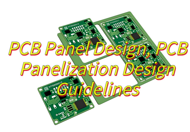
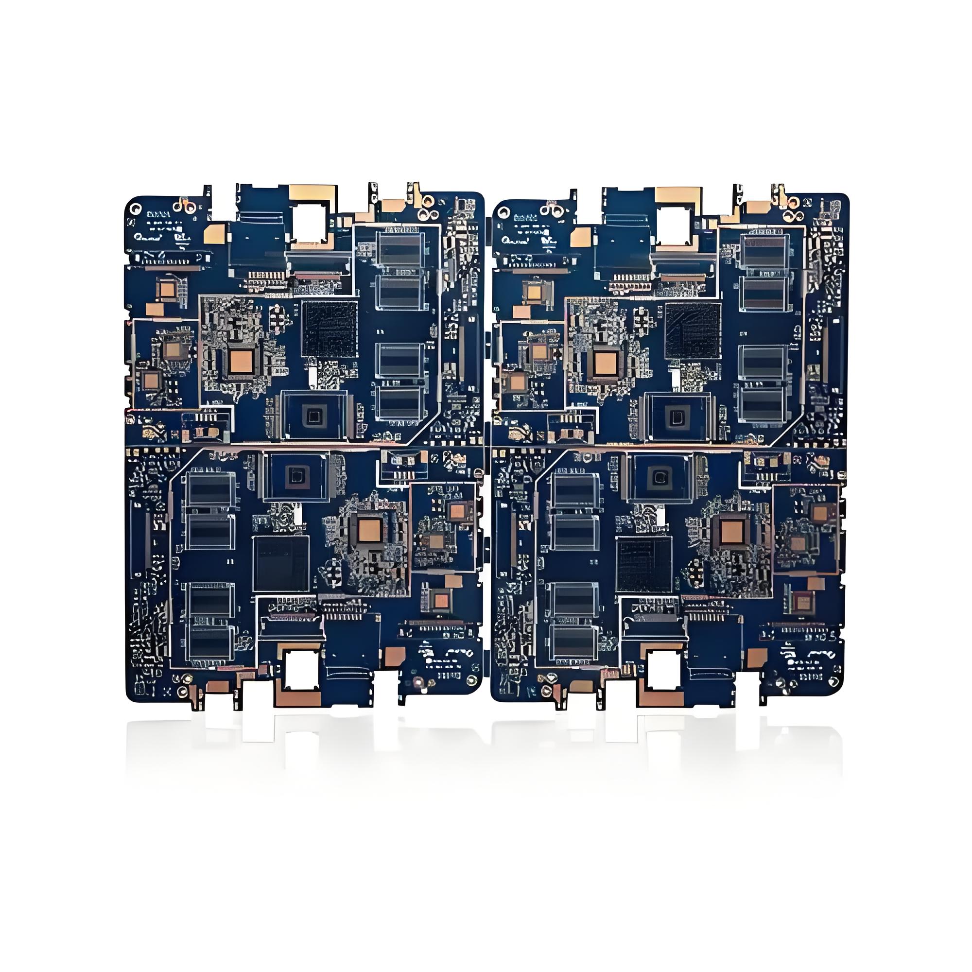
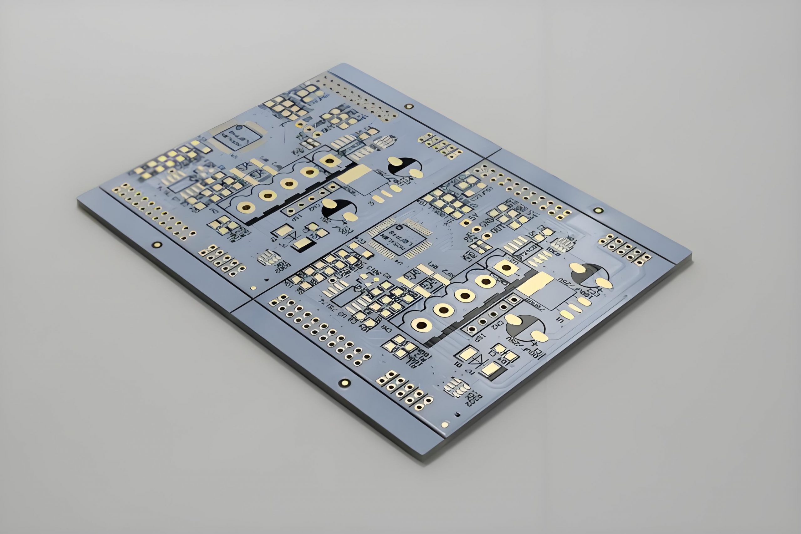
What Is PCB Panel Design?
PCB panel design is the strategic process of arranging multiple printed circuit boards onto a single manufacturing panel to optimize production efficiency while ensuring structural integrity and assembly compatibility. This essential practice in PCB panelization design guidelines involves carefully spacing individual boards with breakaway tabs, routing channels, or perforated connections that allow clean separation after component assembly, while incorporating tooling holes, fiducials, and clearance margins to facilitate automated handling during fabrication. The effectiveness of PCB panel design directly impacts material utilization, manufacturing yield, and depaneling reliability, requiring balanced consideration of board spacing, panel thickness, and breakaway method selection to prevent stress fractures or component damage. Proper PCB panel design follows industry-proven layouts that account for thermal expansion during soldering, mechanical stress during depaneling, and alignment precision for high-density interconnects, making it a foundational element in mass production workflows where even minor miscalculations in panelization can cascade into significant quality issues. Following established PCB panelization design guidelines ensures that the transition from design files to mass-produced boards maintains dimensional accuracy and functional reliability across the entire manufacturing cycle.
Why Do PCB Panel Design?
Here are the practical benefits of PCB panel design explained with clear business advantages:
- Cost Efficiency in Manufacturing: PCB panel design allows multiple boards to be produced simultaneously on a single panel, reducing material waste and optimizing production time. This directly lowers per-unit manufacturing costs while maintaining quality standards.
- Improved Assembly Reliability: Following PCB panelization design guidelines ensures stable board handling during automated assembly. The panel structure prevents warping and misalignment during soldering, reducing costly defects.
- Enhanced Testing Efficiency: PCB panel design enables batch testing of multiple boards at once, cutting quality control time by up to 50% compared to individual board testing. This accelerates time-to-market while maintaining defect detection accuracy.
- Material Utilization Optimization: Strategic board arrangement within panels minimizes substrate waste. Proper PCB panelization design guidelines help utilize up to 95% of raw material, significantly reducing procurement expenses.
- Logistics and Handling Savings: Standardized panel sizes simplify packaging and transportation, decreasing shipping damage risks and storage requirements. This creates measurable savings in supply chain operations.
- Thermal Process Stability: PCB panel design ensures even heat distribution during reflow soldering, preventing localized overheating that could compromise solder joints. This improves long-term product reliability.
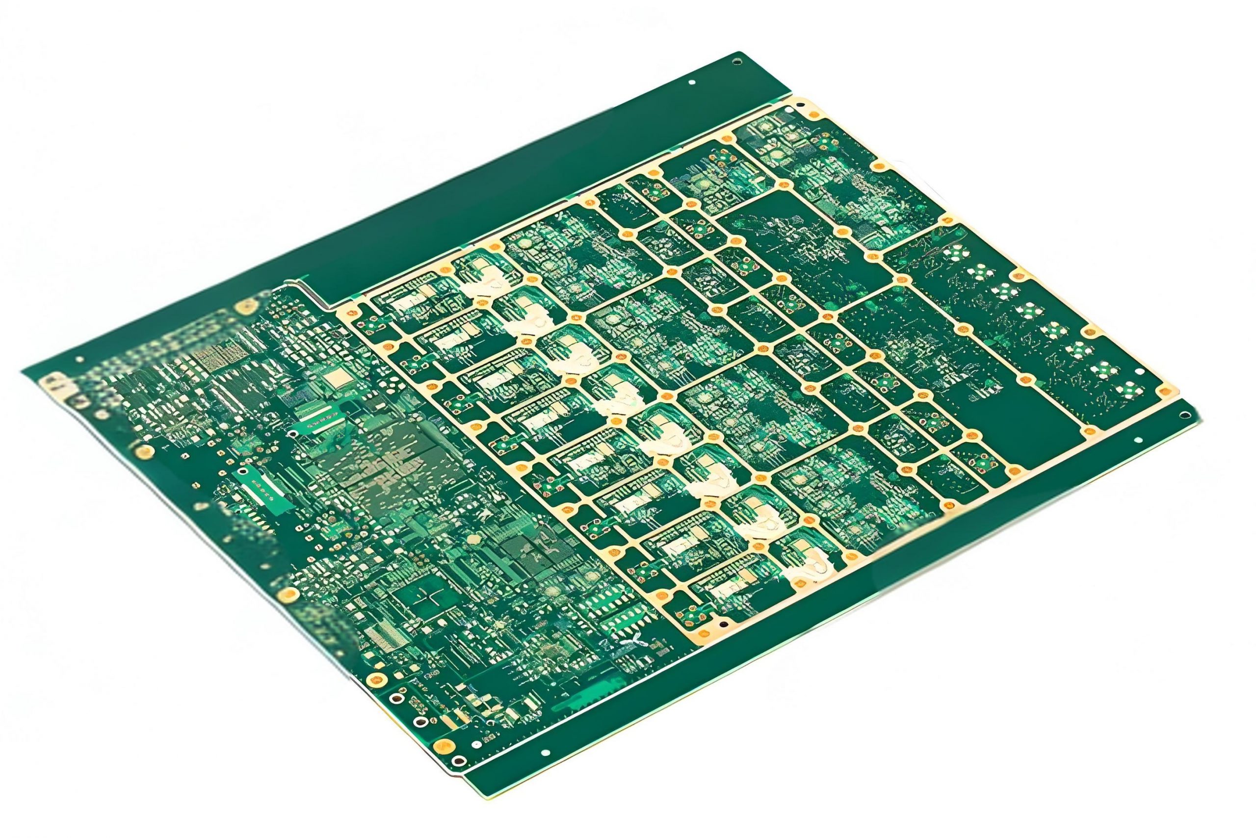
What Are the Different Types of PCB Panels?
Here are the primary types of PCB panels used in manufacturing, each offering distinct advantages for cost and production efficiency:
Single-Unit Panel
- Contains identical PCBs arranged uniformly
- Maximizes material usage when producing high volumes of the same design
- Simplifies assembly line processes through standardized handling
Mixed Panel (Multi-Circuit Panel)
- Combines different PCB designs on one panel
- Ideal for low-volume production of varied products
- Reduces setup costs by processing multiple designs simultaneously
Breakaway Tab Panel (Tab-Routed Panel)
- Uses small perforated tabs to connect individual boards
- Allows manual separation without specialized equipment
- Cost-effective for prototypes and small batches
V-Scored Panel
- Features V-shaped grooves between boards for clean separation
- Enables high-speed depaneling with minimal stress on components
- Reduces material waste compared to routing
Plated Half-Cut Panel
- Incorporates partially cut copper connections between boards
- Provides electrical continuity during testing while allowing easy breakage
- Lowers testing costs through panel-level verification
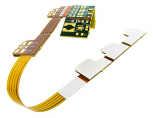
Flexible Panel (Rigid-Flex Panel)
- Combines rigid and flexible sections in one panel
- Eliminates connectors between board segments
- Reduces assembly time and improves reliability in complex designs
How to Design A PCB Panel?
Designing an efficient PCB panel requires balancing functionality, manufacturability, and cost efficiency. Below is a structured, step-by-step approach to creating a panel layout that reduces expenses, accelerates production, and ensures reliability.
1. Optimize Panel Layout and Material Usage
- Maximize Board Density: Arrange PCBs within standard panel sizes (e.g., 18×24 inches) using design software to minimize unused space. Combine small and large boards or rotate irregular shapes to fill gaps.
- Benefit: Reduces material waste by up to 35%, lowering per-unit costs.
- Standardize Orientation: Align all boards in the same direction to simplify automated assembly processes, reducing machine setup time.
2. Incorporate Robust Tooling Rails
- Design Sturdy Rails: Add 5–10mm-wide rails along panel edges to provide structural stability during handling and manufacturing.
- Benefit: Prevents panel warpage, ensuring consistent drilling and soldering quality.
- Add Fiducial Markers: Place 1mm-diameter copper fiducials on rails to guide automated optical inspection (AOI) and component placement machines.
3. Engineer Breakaway Tabs and Separation Features
- Strategic Tab Placement: Use 2–3mm tabs to connect individual PCBs. Avoid placing tabs near delicate components or high-density trace areas.
- Benefit: Enables easy depanelization without damaging boards, reducing labor costs.
- Include V-Scoring or Perforations: Add V-shaped grooves or perforated lines between boards for clean, stress-free separation.
4. Address Thermal and Mechanical Stress
- Stress Relief Design: Integrate slots or cutouts near heavy components (e.g., connectors) to prevent panel distortion during reflow soldering.
- Benefit: Reduces soldering defects and rework expenses.
- Thermal Management: Distribute thermal vias around heat-sensitive components to improve heat dissipation and maintain temperature uniformity.
5. Streamline Testing and Traceability
- Universal Test Points: Align test pads (e.g., 1mm gold-plated copper) across all boards for efficient in-circuit testing (ICT).
- Benefit: Accelerates quality control, reducing test time by up to 40%.
- Identification Markers: Include QR codes, batch numbers, or part numbers on rails for easy traceability during assembly and shipping.
6. Validate with Design for Manufacturability (DFM) Tools
- Run Simulations: Use DFM software to detect issues like insufficient spacing, improper tab placement, or non-compliant drill sizes.
- Benefit: Prevents costly redesigns and ensures first-pass success.
- Prototype Testing: Produce a small batch to validate assembly processes and identify bottlenecks before full-scale production.
7. Finalize Comprehensive Documentation
- Detailed Panel Drawings: Include dimensions, tab locations, and scoring specifications in manufacturing files.
- Benefit: Ensures consistency across batches and reduces supplier miscommunication.
- Supplier Guidelines: Provide clear instructions on depanelization methods (e.g., manual vs. automated) to avoid misinterpretation.
What Are the Commonly Used PCB Panelization Design Software?
Selecting the right software can significantly streamline the PCB panelization process, ensuring efficiency, accuracy, and cost-effectiveness. Below is a curated list of widely used tools, each offering unique features to address different design needs:
Altium Designer
- Core Strengths: Seamlessly integrates panelization tools with its PCB design ecosystem. Features include automated panel layout wizards, real-time 3D visualization, and built-in design rule checks (DRC) to prevent errors.
- Why It Stands Out: Ideal for complex, high-density boards. Its rule-driven engine ensures consistent spacing and alignment across panels, reducing rework.
Cadence Allegro
- Core Strengths: Specializes in advanced panelization for high-speed and RF designs. Offers dynamic array optimization and embedded thermal/mechanical stress analysis.
- Why It Stands Out: Critical for applications requiring signal integrity, such as 5G or automotive electronics. Its simulation tools predict panel behavior under thermal cycling.
Mentor Graphics PADS
- Core Strengths: Combines auto-routing with panel-specific features like tab design and scoring line generation. Includes DFM validation to catch issues early.
- Why It Stands Out: User-friendly for mid-sized teams. Its cost-effective licensing makes it popular for consumer electronics and IoT devices.
Zuken CR-8000
- Core Strengths: Excels in multi-board panelization with 3D MCAD co-design. Supports thermal simulation and mechanical stress analysis for large panels.
- Why It Stands Out: Perfect for aerospace or industrial projects where electrical and mechanical teams collaborate closely.
KiCad (Open Source)
- Core Strengths: Free, open-source tool with basic panelization support. Includes edge cuts, tooling holes, and fiducial markers via its Pcbnew editor.
- Why It Stands Out: A budget-friendly option for startups or hobbyists. Active community forums provide tutorials and troubleshooting.
AutoCAD Electrical
- Core Strengths: Flexible for custom panel shapes. Exports DXF/DWG files for seamless integration with manufacturing equipment.
- Why It Stands Out: Useful for non-standard layouts or legacy systems requiring CAD compatibility.
Valor NPI (Siemens)
- Core Strengths: Advanced DFM software focusing on manufacturability. Analyzes solder paste stencils, test points, and cost drivers.
- Why It Stands Out: Reduces prototyping cycles by 50% through predictive analytics, saving time and money.
What Is the Basic Rule of PCB Panelization Design?
Creating an effective PCB panel requires adherence to foundational rules that ensure manufacturability, cost efficiency, and reliability. Below are the essential guidelines to optimize your panelization design:
- Uniform Board Orientation
- Rule: Align all PCBs consistently in one direction.
- Why: Simplifies automated assembly (e.g., pick-and-place machines), reduces setup time, and minimizes placement errors.
- Impact: Lowers labor costs and accelerates production throughput.
- Maximize Panel Utilization
- Rule: Arrange boards to minimize empty space within standard panel sizes (e.g., 18×24 inches).
- Why: Reduces material waste and cuts raw material costs by up to 30%.
- Impact: Directly lowers per-unit production expenses and supports sustainability.
- Robust Tooling Rails
- Rule: Include 5–10mm-wide rails along panel edges.
- Why: Provides structural stability during drilling, soldering, and handling.
- Impact: Prevents panel warpage and ensures precise component alignment.
- Strategic Breakaway Tabs
- Rule: Connect boards with 2–3mm tabs, avoiding sensitive component areas.
- Why: Enables easy, damage-free separation post-production.
- Impact: Reduces labor costs and scrap rates during depanelization.
- V-Scoring or Perforations
- Rule: Add V-shaped grooves or perforated lines between boards.
- Why: Facilitates clean, stress-free separation without mechanical damage.
- Impact: Ensures boards detach smoothly, maintaining edge quality.
- Thermal and Mechanical Stress Relief
- Rule: Integrate stress-relief features (e.g., slots) near heavy components (e.g., connectors).
- Why: Prevents panel distortion during high-temperature processes like reflow soldering.
- Impact: Reduces soldering defects and rework, improving first-pass yield.
- Design for Manufacturability (DFM) Validation
- Rule: Use DFM tools to check for issues like insufficient spacing or non-compliant drill sizes.
- Why: Identifies and resolves design flaws early, preventing costly redesigns.
- Impact: Reduces prototyping iterations and ensures smooth, error-free production.
How to Evaluate the Rationality of PCB Panelization Design?
Below are methods about how to evaluate the rationality of PCB panelization design:
- Material Utilization Rate
- Metric: Calculate the ratio of usable PCB area to total panel area.
- Evaluation: Aim for ≥85% utilization. Lower rates indicate inefficient layout design.
- Impact: Directly reduces material waste and lowers production costs.
- Manufacturing Throughput
- Metric: Measure the time required for assembly, soldering, and testing per panel.
- Evaluation: Streamlined designs minimize machine downtime and enable parallel processing.
- Impact: Accelerates production, reducing labor costs and time-to-market.
- Depanelization Ease
- Metric: Assess the simplicity of breaking tabs or scoring lines.
- Evaluation: Designs with clean V-scoring or perforations reduce labor and damage risks.
- Impact: Simplifies post-production processes and minimizes scrap.
- Structural Stability
- Metric: Verify the inclusion of tooling rails (5–10mm width) and fiducial markers.
- Evaluation: Rails prevent warpage; fiducials ensure precise alignment with automated systems.
- Impact: Improves yield and reduces rework during assembly.
- Thermal and Mechanical Compliance
- Metric: Analyze stress-relief features near heavy components (e.g., slots, thermal vias).
- Evaluation: Ensure designs withstand reflow soldering without distortion.
- Impact: Reduces soldering defects and enhances reliability.
- Testability and Traceability
- Metric: Check for standardized test points (e.g., 1mm gold-plated pads) and QR codes.
- Evaluation: Test points must align across all boards for efficient in-circuit testing (ICT).
- Impact: Streamlines quality control and simplifies defect tracking.
- Cost-Benefit Ratio
- Metric: Compare total production costs (material, labor, rework) against savings from panelization.
- Evaluation: Aim for a 15–30% cost reduction per unit compared to single-board production.
- Impact: Ensures a positive return on investment (ROI) for panelization efforts.
Should I Design Panels in My PCB Gerber?
No, you should not design panels directly within your PCB Gerber files. Gerber files are intended to define the individual board’s layout—traces, pads, and layers—while panelization is a manufacturing optimization step best handled separately. Including panelization details like tooling holes, scoring lines, or board arrays in Gerbers risks confusing fabricators, as they expect single-board definitions. Instead, provide a dedicated panelization drawing alongside your Gerber files to specify requirements such as board quantity per panel, spacing, tab placement, and fiducial locations. This approach allows manufacturers to adapt the panel layout to their equipment (e.g., panel size limits, drilling capabilities) while ensuring your design intent is respected. Embedding panelization in Gerbers may also lead to errors, such as accidental inclusion of panel-specific features in the final PCBs. By separating panelization guidelines from core design data, you maintain clarity in the Gerber files and empower manufacturers to optimize production for cost efficiency and quality. Always confirm with your fabricator that they accept panelization instructions as a standalone document to streamline collaboration and avoid misinterpretation.