A PCB stencil is a precision-cut template used to print solder paste onto PCB pads before SMT component placement. Its apertures control where solder paste is deposited and how much paste reaches each pad. Stencil thickness, aperture geometry, material, and printing conditions affect paste transfer efficiency and solder-joint quality. This guide explains PCB stencil types, material selection, thickness, area ratio calculations, step stencil design, printing defects, and how to prepare manufacturing files for reliable PCB assembly.
At EBest Circuit, we coordinate PCB fabrication, stencil preparation, component sourcing, and SMT assembly through one manufacturing team. Our Free DFM, No MOQ, 4 SMT lines, and dedicated support from 1 sales representative + 3 engineers help customers resolve aperture design, component footprint, and solder paste printing concerns before production. Send your Gerber files, BOM, assembly drawings, and quantities to sales@bestpcbs.com for a project-specific manufacturing review and quotation.
Key Takeaways
- A PCB stencil transfers solder paste onto SMT pads through precisely cut apertures. It controls deposit position and volume before component placement.
- Stainless steel is the most widely used SMT stencil material. Laser cutting produces accurate apertures, while electropolishing and suitable coatings can improve paste release.
- Common stencil thicknesses range from 0.08 mm to 0.20 mm. Selection depends on the smallest apertures, component packages, required solder volume, and printing conditions.
- Stencil area ratio measures aperture opening area relative to its wall area. A ratio of approximately 0.66 or higher is a common starting guideline for conventional solder paste printing.
- Framed stencils are commonly used for repeated automated printing, while frameless stencils offer flexible mounting options for prototypes and compatible printing systems.
- Step-up stencils increase local foil thickness, while step-down stencils reduce it. Both help manage different solder paste volume requirements on the same PCB.
- SPI detects insufficient paste, excessive deposits, bridging, and printing offsets. Measured paste volume and position can help identify stencil or printing process problems.
- Custom PCB stencil manufacturing requires accurate paste-layer data, board dimensions, thickness, and mounting specifications. BOM and assembly drawings help engineers verify special aperture requirements.
What Is a PCB Stencil and What Is It Used For?
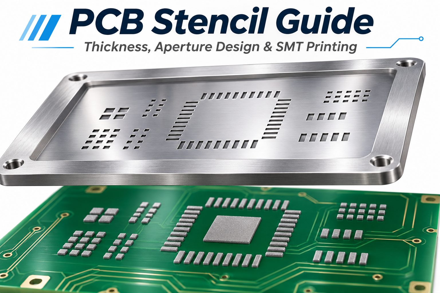
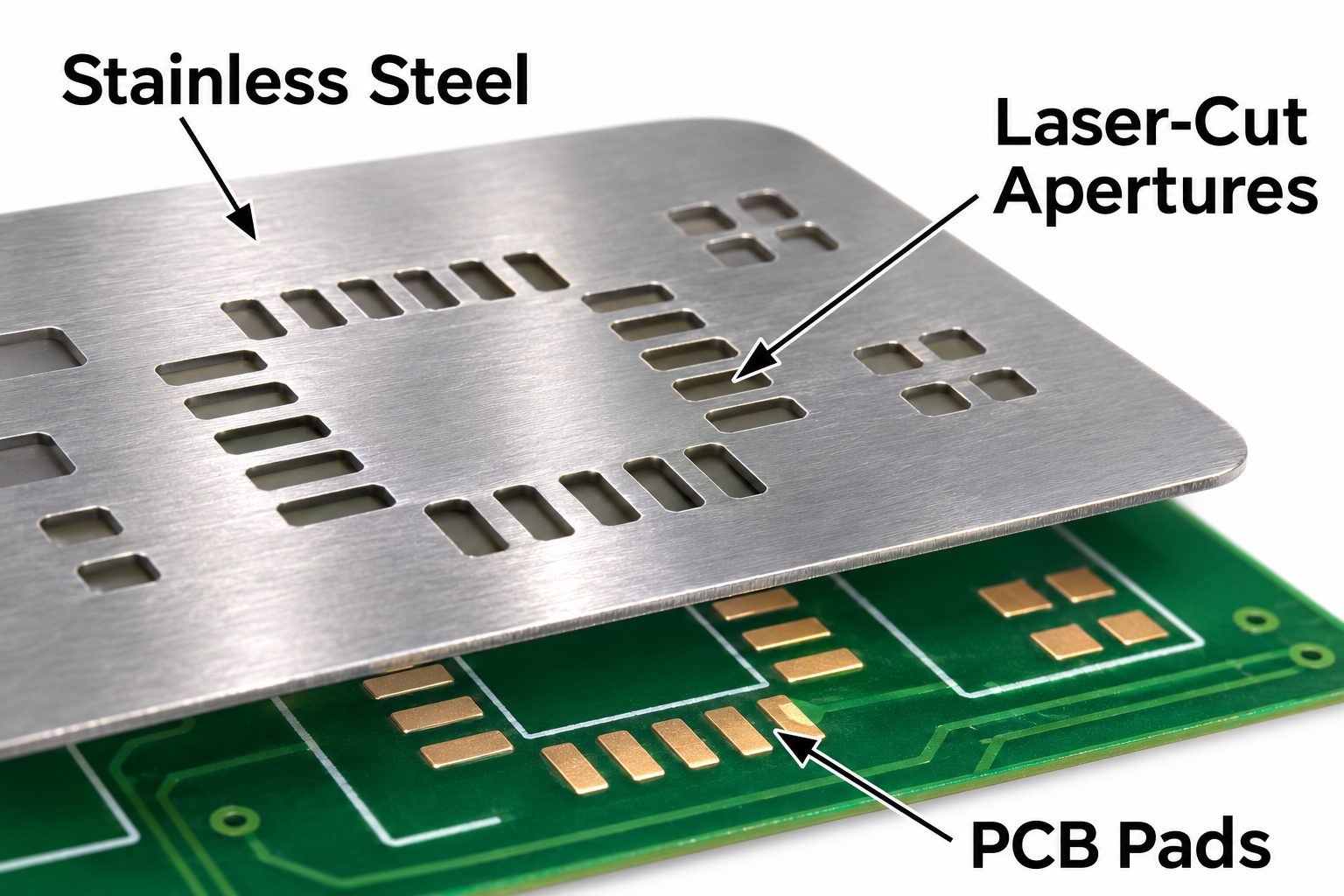
A PCB stencil is a thin, precision-cut sheet used to deposit solder paste onto selected PCB pads before surface-mount assembly. Its openings match the intended paste locations, allowing many solder paste deposits to be printed in one operation.
A typical SMT stencil contains:
- Stencil Foil: Stainless steel or another suitable material containing the apertures.
- Apertures: Openings that define the paste deposit pattern.
- Frame or Holder: Supports the foil during printing.
- Alignment Features: Help position the stencil relative to the PCB.
- Tensioning System: Maintains foil flatness and stability where required.
For a PCB containing hundreds of SMT pads, a stencil allows solder paste to be deposited across the board in a single printing cycle. Accurate aperture positioning helps components sit correctly on their pads during placement and reflow.
The stencil and PCB solder mask serve different purposes. Solder mask defines the exposed copper areas, while the stencil determines the solder paste pattern. The stencil opening may be smaller than the corresponding copper pad when reduced paste volume is required.
Fine-pitch ICs, QFN packages, BGAs, and mixed-component boards often need aperture adjustments rather than a direct copy of every pad outline.
How Does PCB Stencil Printing Work in SMT Assembly?
PCB stencil printing transfers solder paste through aligned stencil apertures using a squeegee, followed by controlled stencil separation. The resulting deposits are inspected before component placement.
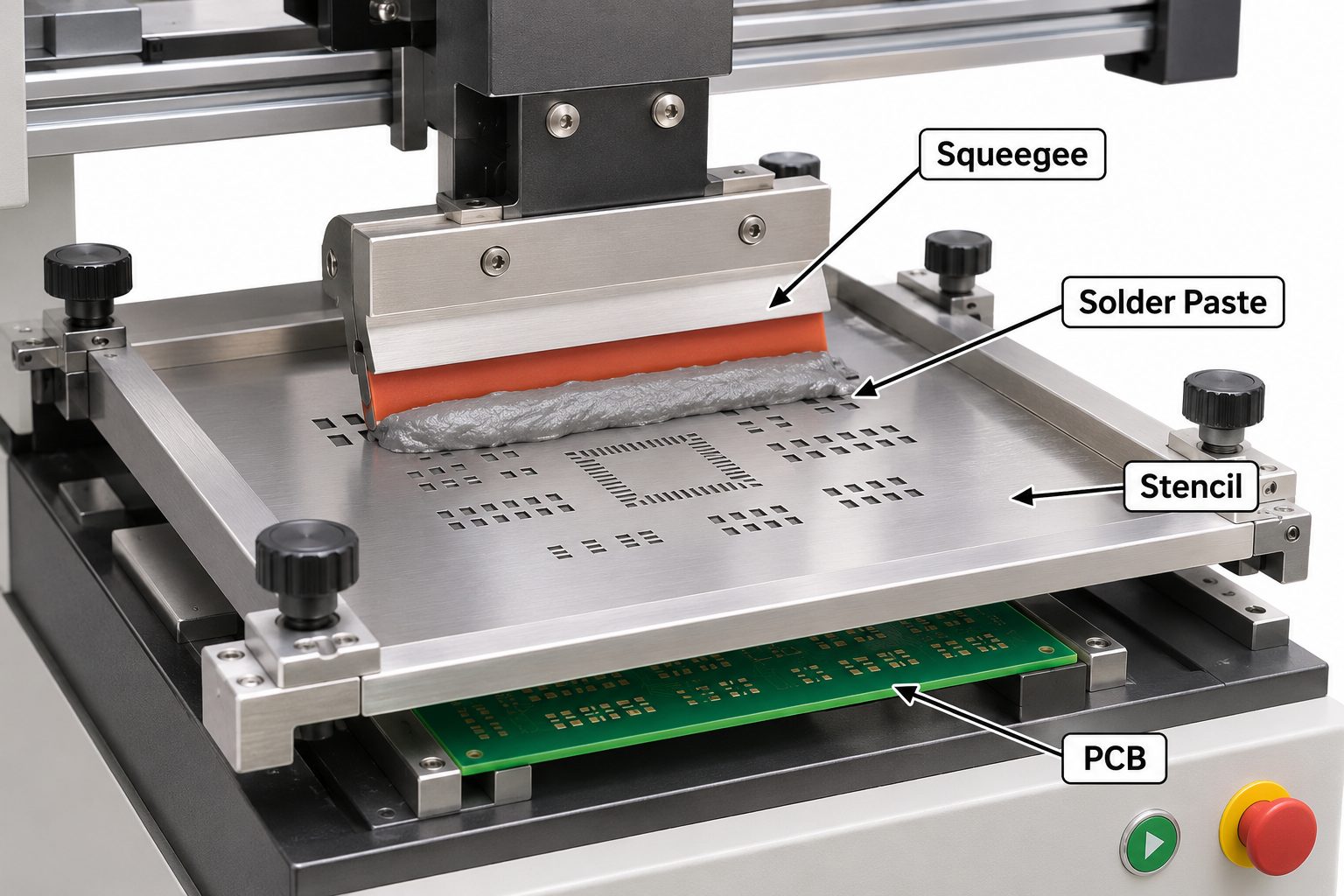
The standard printing sequence includes 5 steps:
- PCB Loading and Support: The PCB is positioned and supported in the printer to limit movement or flexing.
- Stencil Alignment: The printer aligns stencil apertures with PCB pads, commonly using fiducial recognition.
- Solder Paste Printing: A squeegee rolls solder paste across the foil and fills the apertures.
- Stencil Separation: The PCB separates from the stencil, leaving solder paste deposits on the pads.
- Solder Paste Inspection: SPI checks deposit volume, height, area, and position against defined limits.
What Affects Solder Paste Release?
Aperture geometry is important, but the entire printing process determines how much paste reaches the PCB.
Key variables include:
- Stencil Thickness: Influences theoretical paste volume and aperture wall area.
- Aperture Geometry: Affects paste release and deposit shape.
- Squeegee Pressure and Speed: Control aperture filling and paste movement.
- Stencil Separation: Influences deposit transfer from aperture walls.
- PCB Support: Helps maintain consistent stencil-to-board contact.
- Solder Paste Condition: Includes paste type, viscosity, particle size, and handling conditions.
For example, a narrow aperture in a thick stencil may retain more solder paste during separation. Increasing squeegee pressure alone may not correct the problem if aperture release is the primary limitation.
Printing settings, stencil geometry, and SPI measurements should therefore be evaluated together before modifying the process.
What Are the Different Types of PCB Stencils?
PCB stencils are commonly classified by mounting method, application, and foil construction. Framed and frameless stencils describe mounting arrangements, while step stencils and rework stencils address particular manufacturing requirements.
| Stencil Type | Main Characteristic | Typical Use |
|---|---|---|
| Framed | Foil mounted in rigid frame | Repeat SMT production |
| Frameless | Separate compatible holder | Prototype / flexible runs |
| Prototype | Simplified mounting | Engineering samples |
| Step Stencil | Locally varied thickness | Mixed-component PCBs |
| Rework Stencil | Localized paste pattern | Component replacement |
Framed Stencils
Framed stencils provide a stable assembly for repeated use in compatible SMT printing equipment. The foil is mounted with controlled tension, helping maintain its position and flatness during production.
Frameless Stencils
Frameless stencils are used with a separate holder, tensioning system, or suitable fixture. They offer flexibility when several stencil designs share compatible equipment.
Prototype Stencils
Prototype stencils are commonly used for engineering samples and limited production quantities. Their mounting may be simpler, but fine-pitch apertures still require accurate dimensions and alignment.
Step Stencils
Step stencils incorporate local foil thickness changes to control solder paste volume in selected regions. They are useful when one uniform thickness cannot adequately serve all component types.
Rework Stencils
Rework stencils apply solder paste to localized component areas during repair or replacement. Their dimensions must match the specific component and rework method.
These categories can overlap. For example, a stencil may be stainless steel, laser-cut, framed, and step-down at the same time.
What Materials Are Used to Manufacture PCB Stencils?
Stainless steel is the standard material for most commercial SMT stencils because it offers durability, dimensional stability, and compatibility with precision manufacturing. Electroformed nickel and selected polymer materials serve more specialized applications.
| Material | Main Advantage | Consideration |
|---|---|---|
| Stainless Steel | Durable and widely available | Standard SMT choice |
| Electroformed Nickel | Fine-feature capability | Process-dependent cost |
| Polymer Film | Convenient for prototypes | Limited durability |
Stainless Steel
Stainless steel, including suitable 304-grade material, is widely used for production stencils. It supports repeated printing and can be manufactured in thin foil sizes for fine-pitch applications. Common nominal thicknesses include 0.08, 0.10, 0.12, 0.15, and 0.20 mm, depending on supplier capability.
Electroformed Nickel
Electroformed nickel can provide precise aperture geometry and favorable wall characteristics for certain small-feature applications. Its suitability depends on aperture dimensions, solder paste behavior, manufacturing requirements, and cost.
Polymer Film
Polymer stencils can be useful for basic prototypes or less demanding printing applications. Their wear resistance and dimensional stability generally make them less suitable for intensive automated SMT production.
How Does Stencil Manufacturing Affect Aperture Quality?
Material selection and aperture manufacturing are separate decisions. Common manufacturing and finishing methods include:
- Laser Cutting: Produces apertures using the approved digital pattern.
- Electroforming: Creates precision foil structures through an electrochemical process.
- Electropolishing: Improves selected aperture wall characteristics.
- Deburring: Removes unwanted material from aperture edges.
- Surface Coating: Can reduce paste adhesion and improve release in suitable applications.
For most standard SMT assemblies, laser-cut stainless steel is a practical starting point. Specialized materials or coatings are worth evaluating when fine-feature printing performance justifies the additional process requirements.
How Do You Choose the Correct PCB Stencil Thickness?
PCB stencil thickness should be selected according to the smallest aperture, required solder paste volume, component pitch, and overall printing requirements. A thicker stencil provides greater theoretical paste volume, while a thinner stencil generally improves release from narrow apertures.
The following values are useful initial references.
| Thickness | Initial Design Consideration |
|---|---|
| 0.08 mm (80 µm) | Very fine apertures |
| 0.10 mm (100 µm) | Fine-pitch components |
| 0.12 mm (120 µm) | Mixed SMT layouts |
| 0.15 mm (150 µm) | General SMT printing |
| 0.20 mm (200 µm) | Larger paste requirements |
These are reference thicknesses rather than fixed rules for specific component packages.
1. How Does Thickness Affect Solder Paste Volume?
For a rectangular opening, theoretical aperture volume is:
Where:
- L = Aperture length.
- W = Aperture width.
- T = Stencil thickness.
Consider a 0.50 mm × 0.80 mm aperture:
| Stencil Thickness | Theoretical Volume |
|---|---|
| 0.10 mm | 0.040 mm³ |
| 0.12 mm | 0.048 mm³ |
| 0.15 mm | 0.060 mm³ |
Increasing thickness from 0.10 mm to 0.15 mm increases theoretical aperture volume by 50%. However, actual deposited volume also depends on transfer efficiency. A deeper aperture can retain more paste along the walls, particularly when its area ratio is low.
2. Fine-Pitch vs Larger Components
Fine-pitch ICs often favor thinner foils or modified aperture patterns because their pad openings are narrow. Larger connectors and power components may require more solder paste to form suitable joints.
For a mixed-component board, review:
- Smallest aperture width and length.
- Required solder volume.
- Component pitch and pad geometry.
- Paste release from the smallest openings.
- Solder paste particle size.
- Printer capability and board support.
The best starting point is a foil thickness that satisfies the smallest critical apertures while providing enough paste for the other components. Where one thickness cannot meet both requirements, a step stencil may be considered.
How Do You Calculate PCB Stencil Aperture Area Ratio?
Stencil aperture area ratio is the aperture opening area divided by its internal wall area. It helps predict solder paste release during stencil separation, especially for small and fine-pitch openings.
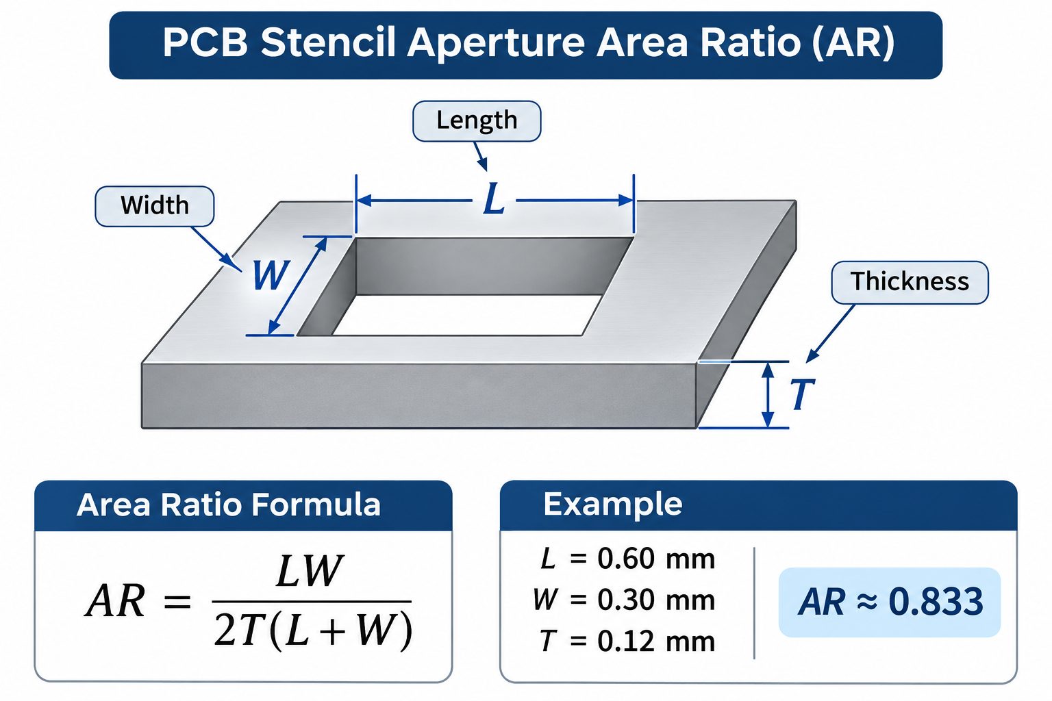
A ratio around 0.66 or higher is a commonly used design starting point, not a guaranteed printing acceptance limit. Actual release depends on aperture wall quality, paste properties, stencil material, and process settings.
1. Rectangular Aperture Area Ratio Formula
For a rectangular aperture:
Where:
- AR = Aperture area ratio.
- L = Aperture length.
- W = Aperture width.
- T = Stencil thickness.
All dimensions must use the same unit.
2. Area Ratio Calculation Example
Assume the following aperture dimensions:
| Parameter | Value |
|---|---|
| Aperture Length (L) | 0.60 mm |
| Aperture Width (W) | 0.30 mm |
| Stencil Thickness (T) | 0.12 mm |
Substitute the values:
The calculated area ratio is 0.833, above the commonly used 0.66 guideline. This suggests a comparatively favorable aperture geometry for conventional printing, although the actual transfer efficiency must be verified through printing results.
3. What Is the Stencil Aspect Ratio?
Aspect ratio compares the aperture’s narrow dimension with foil thickness:
Using the same example:
An aspect ratio around 1.5 or higher is another common design reference. Area ratio generally provides a more complete indication of aperture release geometry because it considers opening area and total wall area.
4. How Can You Improve Paste Release?
When area ratio is too low, consider:
- Reducing foil thickness where solder volume permits.
- Adjusting aperture dimensions within solder-joint requirements.
- Improving aperture wall finish.
- Reviewing paste particle size and printing properties.
- Evaluating suitable coatings or stencil materials.
- Adjusting separation parameters where supported.
The final aperture must still provide enough paste for the intended solder joint.
5. QFN and BGA Aperture Design
Different component packages require different aperture considerations.
QFN Peripheral Pads: Apertures should provide controlled paste volume while maintaining separation between adjacent deposits. Manufacturer-recommended land patterns are the starting point.
QFN Exposed Thermal Pads: Large exposed pads commonly use window-pane aperture patterns to control solder volume and manage component stand-off and voiding.
BGA Pads: BGA aperture design depends on package pitch, PCB pad dimensions, paste properties, and the approved assembly process.
For all 3 cases, solder paste aperture geometry should be reviewed alongside the actual PCB footprint and component manufacturer’s assembly guidance.
When Should You Use a Step-Up or Step-Down PCB Stencil?
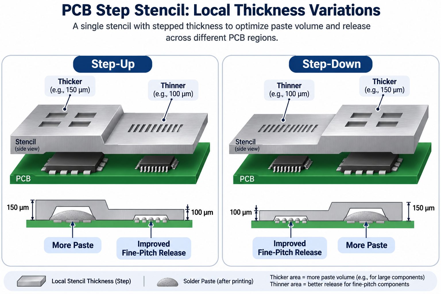
A step stencil is used when different PCB regions require different solder paste volumes that cannot be reliably achieved with a uniform foil thickness. Step-up regions increase thickness locally, while step-down regions reduce it.
| Feature | Step-Up | Step-Down |
|---|---|---|
| Local Thickness | Increased | Reduced |
| Main Purpose | More potential paste | Less paste / improved release |
| Typical Use | Larger solder joints | Fine-pitch components |
| Main Check | Paste volume | Area ratio |
Step-Up Stencil
A step-up region increases foil thickness around selected apertures. For example, a stencil with a 0.12 mm base thickness may use a 0.15 mm local region where a larger paste volume is required. The benefit depends on aperture geometry and effective paste release.
Step-Down Stencil
A step-down region reduces local thickness. For example, a board using 0.15 mm foil may have a fine-pitch area reduced to 0.10 mm to improve paste release or reduce deposits.
Mixed-Component PCB Example
Consider a PCB containing 0.4 mm-pitch ICs, 0402 passives, and a larger shielded connector. The fine-pitch IC may require reduced foil thickness, while the connector needs more solder paste. A step stencil can accommodate both requirements when local geometry and printing equipment permit.
Before approval, check:
- Step height and local foil thickness.
- Aperture distance from step boundaries.
- Squeegee travel direction.
- Printer compatibility.
- Foil support and flatness.
- Paste release in the affected region.
A step stencil adds manufacturing complexity. It should be used when the expected improvement in paste-volume control justifies that complexity.
How Do You Use Framed and Frameless Stencils in SMT Printing?
Framed stencils provide a permanently mounted foil for repeatable printing, while frameless stencils rely on a compatible holder or tensioning system. Both can produce accurate results when properly mounted, aligned, and maintained.
| Feature | Framed | Frameless |
|---|---|---|
| Support | Permanent frame | Separate holder |
| Tension | Established during mounting | Holder-dependent |
| Common Use | Repeat production | Prototype / flexible runs |
| Handling | Rigid assembly | Requires mounting |
| Storage | Larger | More compact |
Framed Stencil Setup
Before printing, verify:
- Frame size matches the printer.
- Foil tension and flatness are acceptable.
- Orientation matches the PCB panel.
- Alignment features are correctly recognized.
- Underside cleaning can be performed.
Framed stencils are convenient for recurring production because the assembled frame can be identified, stored, and reinstalled.
Frameless Stencil Setup
Frameless designs need a compatible holder or suitable fixture. The operator must secure the foil evenly and confirm its alignment with the PCB. Inadequate mounting can introduce movement or inconsistent stencil-to-board contact.
Stencil Maintenance
For both configurations, monitor:
- Paste buildup inside apertures.
- Underside contamination.
- Foil damage.
- Frame or holder condition.
- Changes in paste transfer consistency.
The stencil must match the current PCB revision. Changes to pad locations, footprints, or paste-layer openings may require a new stencil even when the existing foil remains physically usable.
What PCB Stencil Printing Defects Should You Check?
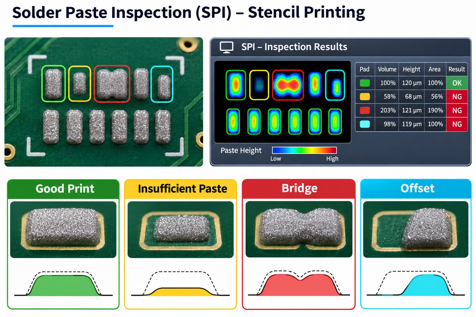
The most common stencil printing defects are insufficient solder paste, excess paste, bridging, printing offsets, and uneven deposits. These problems affect solder-joint formation and should be detected before reflow.
| Defect | Possible Cause | Engineering Check |
|---|---|---|
| Insufficient Paste | Poor release | Area ratio, wall finish |
| Excess Paste | Excess deposit volume | Aperture, thickness |
| Bridging | Overprint or misalignment | Aperture spacing |
| Printing Offset | Registration error | Fiducials, support |
| Uneven Deposits | Process variation | Squeegee, paste, SPI |
1. Insufficient Solder Paste
Insufficient paste can result from incomplete aperture filling or poor release. Typical checks include:
- Area ratio and aperture dimensions.
- Blocked or contaminated apertures.
- Solder paste condition.
- Printing speed and pressure.
- Stencil separation behavior.
A low-volume SPI result does not automatically mean that the aperture is too small. Printing parameters and aperture condition should also be examined.
2. Excess Paste and Bridging
Excess paste increases the risk of solder bridging, solder balls, and uneven joint formation. Review aperture dimensions, stencil thickness, alignment, and paste spread. Fine-pitch components are especially sensitive to excessive deposit width and printing offset.
3. Printing Offset
Printing offset occurs when deposits are displaced from the intended PCB pads. Check fiducial recognition, stencil positioning, board support, and panel movement before changing aperture design.
4. Uneven Deposits
Inconsistent deposits can result from variable contact pressure, poor board support, paste condition, or stencil contamination. SPI measurements help determine whether the variation occurs across the entire board, in one region, or at specific aperture sizes.
What Does SPI Measure?
Three-dimensional solder paste inspection can evaluate:
- Deposit volume.
- Deposit height.
- Deposit area.
- X/Y positional offset.
- Missing or bridged deposits.
- Printing variation across pads.
For example, an aperture with a theoretical volume of 0.048 mm³ and an assumed transfer efficiency of 85% would produce an estimated deposit volume of:
The 85% value is an illustrative assumption, not a universal SPI acceptance threshold. At EBest Circuit, SPI results can help identify printing variation and support engineering reviews of aperture design, stencil condition, and process parameters.
What Files and Specifications Do You Need to Order a PCB Stencil?
Ordering a custom PCB stencil typically requires approved paste-layer data, PCB or panel dimensions, foil thickness, mounting specifications, and any special aperture requirements. Supporting assembly files help engineers confirm the stencil design against the component packages.
1. Stencil Manufacturing Files
| File or Specification | Purpose |
|---|---|
| Gerber Paste Layer | Aperture pattern |
| PCB / Panel Outline | Position and dimensions |
| Stencil Thickness | Foil specification |
| Frame / Holder Dimensions | Printer compatibility |
| Fiducial Information | Alignment |
| Special Aperture Notes | Local modifications |
| Step Requirements | Thickness variations |
A double-sided SMT board may require separate top and bottom stencil patterns. For panelized production, the stencil must match the manufacturing panel rather than an individual PCB outline.
2. Assembly Reference Files
Useful supporting files include:
- BOM with approved MPNs.
- Pick-and-place data.
- Assembly drawing.
- Component package information.
- Solder paste specification.
- PCB revision and quantity.
These documents help identify packages requiring special aperture patterns or different solder volumes.
3. How Should You Compare PCB Stencil Manufacturers?
Compare suppliers using:
- Foil material and thickness availability.
- Aperture accuracy.
- Laser cutting and finishing options.
- Frame and holder compatibility.
- Step stencil capability.
- Engineering and DFM support.
- Quotation, lead time, and delivery arrangements.
For US buyers, cross-border shipping and engineering communication may also influence supplier selection.
4. What Should You Include in an RFQ?
Provide the approved paste layers, PCB dimensions, requested foil thickness, mounting type, quantities, and special requirements. If aperture dimensions or thickness are uncertain, include the assembly drawing and BOM so the manufacturer can review the design before confirming the stencil specification.
Why Choose EBest Circuit for PCB Stencil Manufacturing and Assembly?
EBest Circuit coordinates PCB fabrication, stencil preparation, component sourcing, SMT assembly, and inspection through one manufacturing project. This allows our engineers to review the solder paste design alongside the PCB footprint and assembly requirements before production.
Our capabilities include:
- Free DFM Review: Check paste layers, aperture geometry, stencil thickness, and component footprints.
- Stencil Preparation Support: Review framed, frameless, laser-cut, and step stencil requirements.
- No MOQ: Support prototypes, low-volume validation, and repeat production.
- 4 SMT Lines: 2 JUKI and 2 YAMAHA production lines.
- 01005 Assembly: Support miniature components where the design and process requirements permit.
- Component Sourcing: Coordinate approved electronic components according to the BOM.
- SPI and AOI: Inspect solder paste deposits and assembled boards.
- MES Traceability: Support board-level production record retrieval.
- Engineering Support: 1 sales representative + 3 engineers coordinate reviews and manufacturing requirements.
Our manufacturing operations are supported by applicable quality management certifications, including ISO 9001, ISO 13485, IATF 16949, and AS9100D, with certification scope available for supplier qualification.
For a custom PCB stencil, framed SMT stencil, step stencil, or complete PCB assembly project, send your Gerber files, paste layers, BOM, assembly drawings, quantities, and manufacturing requirements to sales@bestpcbs.com. Our engineering team can review your design and provide a project-specific quotation.
Frequently Asked Questions About PCB Stencils
1. Can I use the same PCB stencil for multiple production runs?
Yes. A stainless steel stencil can be reused when it remains flat, clean, undamaged, and compatible with the current PCB revision. Inspect aperture walls, foil tension, frame condition, and paste release before reuse. Changes to pad locations or paste-layer geometry may require a new stencil.
2. Can a PCB stencil be made with a 3D printer?
Yes, certain 3D printing methods can produce prototype stencil-like templates. However, fine aperture accuracy, surface finish, and durability may be limited. Laser-cut stainless steel is generally more suitable for repeatable SMT printing and fine-pitch assemblies.
3. Can I use a DIY PCB stencil for 0402 or fine-pitch ICs?
A DIY stencil may work for some 0402 or fine-pitch components if aperture size, foil thickness, and alignment are sufficiently accurate. Repeatable printing becomes more difficult as apertures shrink. Professionally manufactured stencils offer greater control for production and demanding assemblies.
4. Does every PCB assembly project need a solder paste stencil?
No. Automated SMT assembly commonly uses stencil printing, but some prototypes can be assembled using manually dispensed solder paste or other suitable methods. Stencils become especially useful when the board contains many SMT pads or repeatable paste volume is required.
5. Can the same stencil be used for leaded and lead-free solder paste?
Yes, the same stencil may be suitable when aperture geometry and printing requirements are compatible. Solder paste formulations differ in particle size distribution, flux chemistry, and rheology, so printing parameters may need adjustment. The process should be validated for each paste type.
6. How often should an SMT stencil be cleaned?
Cleaning frequency depends on aperture size, solder paste, printing conditions, and inspection results. Fine-pitch designs may require more frequent underside cleaning. Establish the interval from paste transfer consistency, contamination, and SPI data rather than using one fixed print count.
7. What HS code applies to PCB solder paste stencils?
PCB solder paste stencils do not have one universally applicable HS code without reviewing their material, construction, and importing country. The supplier and importer should confirm classification against the current customs tariff schedule and supporting product documents before shipment.
Conclusion
A PCB stencil controls solder paste placement and volume during SMT assembly. Stencil thickness, aperture area ratio, material, and printing conditions influence paste transfer efficiency and solder-joint quality, while step stencils help manage different solder-volume requirements on one board. SPI provides measurable feedback to identify printing defects before reflow. EBest Circuit supports PCB stencil and assembly projects with Free DFM, stencil preparation, PCB fabrication, component sourcing, 4 SMT lines, and inspection services. Send your manufacturing files and BOM to sales@bestpcbs.com for an engineering review and quotation.