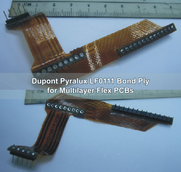
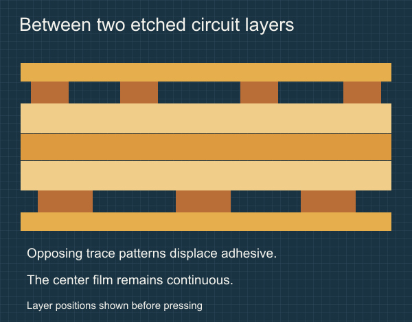
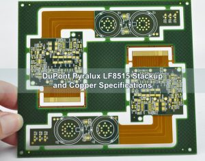
Dupont Pyralux LF0111 bonds two etched circuit layers together. It consists of a 25 µm Kapton® polyimide film with 25 µm of B-staged modified acrylic adhesive on each side. The two adhesive faces fill around the facing copper patterns during lamination, while the central film provides a continuous dielectric barrier. The copper belongs to the adjoining circuit layers; LF0111 itself contains no foil.
Where Does LF0111 Go in a Flex PCB Stackup?
Place LF0111 between two patterned faces that need to be bonded and electrically isolated. In a multilayer PCB, each adhesive face contacts a separate circuit layer. That lets one bond ply encapsulate both etched patterns. A copper-clad core such as Pyralux LF8515R serves a different purpose: it supplies foil for forming traces.
For a rigid-flex board, mark the areas where the layers must be bonded and any area intended to flex with separate, unbonded leaves. Extending the bond ply across that free-flex region changes how the leaves move. A layer list alone cannot show where the bond boundary falls; put the outline on the mechanical drawing.
What Are the LF0111 Material Specifications?
DuPont identifies LF0111 by name in Tables 1 and 2 of its Pyralux LF Bond Ply datasheet (EI-10116). Table 1 describes the material construction. Table 2 gives typical laboratory measurements for LF0111. Use the test frequency and method alongside the value when comparing materials.
| Feature or property | LF0111 value | Condition or interpretation |
|---|---|---|
| Adhesive / Kapton / adhesive | 25 / 25 / 25 µm (1 / 1 / 1 mil) | Nominal incoming layers; count both adhesive faces. |
| Dielectric constant (Dk) | 3.6 at 1 MHz; 3.0 at 10 GHz | IPC-TM-650 2.5.5.3 at 1 MHz; ASTM D2520 at 10 GHz. |
| Loss tangent (Df) | 0.020 at 1 MHz; 0.017 at 10 GHz | Same respective test methods as Dk. |
| Adhesive flow | 0.05–0.10 mm | Typical test result under IPC-TM-650 2.3.17.1. |
| Peel strength to copper | 1.8 N/mm as received; 1.6 N/mm after solder | IPC-TM-650 2.4.9 on a prepared copper specimen. |
How Does Adhesive Fill Around Copper Traces?
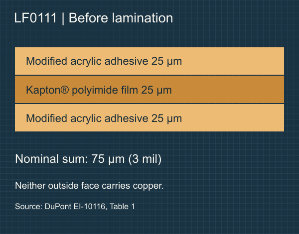
Before pressing, the raised copper traces touch the bond ply first. Between traces, the exposed substrate lies lower. As the adhesive heats and flows, some of it fills that relief. A sparsely routed area and an adjacent solid plane can therefore place different demands on the same adhesive face. The opposite face encounters its own copper pattern.
Show both facing artwork layers and the copper thickness at bonding. If an adhesive edge lies near an exposed pad, also dimension the area that must stay clear. The datasheet’s flow test gives a comparison value under a defined method. Using 0.10 mm as a universal pad setback would skip the effects of local copper distribution and the actual press process.
How Thick Is LF0111 After Lamination?
Adding the three incoming layers gives a nominal 3 mil, or about 75 µm using the rounded metric values in the datasheet. To see why that number cannot specify every finished gap, consider two locations on the same board: one where wide copper features face each other, and one where a trace faces an etched opening. The amount of adhesive needed beside the copper differs, as does the pair of surfaces from which you would measure.
If an impedance-controlled PCB requires a particular trace-to-plane spacing, identify those two copper surfaces on the cross-section. Give the target, tolerance and measurement location. The fabricator can then model the cured stackup and agree on a representative coupon. A nominal bond-ply thickness and a frequency-specific Dk are inputs to that review; neither establishes the impedance of a finished trace.
LF0111 Bond Ply vs LF0110 Coverlay
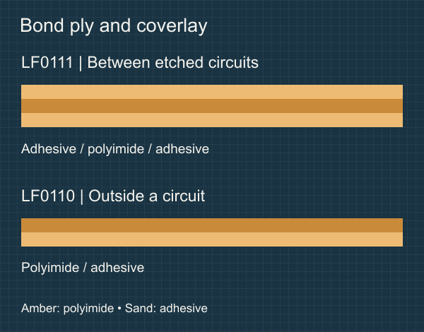
Both codes include Kapton film and modified acrylic adhesive. The decisive difference is the second adhesive face. DuPont’s LF coverlay datasheet, Table 1 identifies LF0110 as 25 µm of film with 25 µm of adhesive on one face. Substituting it between etched layers would leave one interface without the specified adhesive.
| Drawing requirement | LF0111 bond ply | LF0110 coverlay |
|---|---|---|
| Layer sequence | Adhesive / polyimide / adhesive | Polyimide / adhesive |
| Where it belongs | Between circuit details that must bond | On an outside circuit face, with film facing outward |
| Nominal sum before pressing | 75 µm (3 mil) | 50 µm (2 mil) |
| Artwork to supply | Bonded area, cutouts and any no-bond region | Pad and contact openings, edge clearances |
What Lamination Conditions Does DuPont List?
DuPont lists typical LF processing ranges of 182–199 °C part temperature, 14–28 kg/cm² pressure (200–400 psi) and one to two hours at temperature. The dwell refers to time at part temperature. A press platen reaching its setpoint does not by itself establish that the center of the stack has reached the same temperature.
For example, the peel-test footnote specifies a narrower setup: 182 °C, 200 psi and one hour, bonded to the treated side of 1 oz rolled-annealed copper. That footnote explains the peel specimen. The manufacturing cycle for a different layup should be qualified for that stack, copper surface and press equipment.
How Can You Check the Bonded Interface?
Choose a section through a feature that exercises the bond: for example, a broad copper region next to isolated traces or the edge of a cutout near a pad. A cross-section there can show whether adhesive filled the trace shoulders, whether a void remains, and whether material entered a keep-clear area. Mark the inspection location before lamination so the sample corresponds to the feature of interest.
If the application requires a peel test, define the specimen, foil treatment, conditioning and acceptance limit separately. A passing cross-section does not supply a peel-force result. Likewise, a datasheet peel value for treated copper does not verify bonding to a different surface on a finished board.
How Should LF0111 Be Stored?
DuPont specifies original packaging, 4–29 °C and less than 70% relative humidity. Keep the material dry and protected and avoid freezing. Preserve the package label so the material code, batch and quantity can be tied to the production job.
The datasheet ties its stated two-year warranty period to the date on the Certificate of Analysis, subject to the storage conditions. For material transferred from a partial roll, retain the original lot reference and handling record. Warehouse receipt date alone does not establish the certificate date or the roll’s storage history.
What Affects the Price of an LF0111 Flex PCB?
An LF0111 roll price and the price of a finished circuit cover different things. When we estimate board cost, we look at how many circuits fit on a production panel. A narrow bonded strip on each finished board can still require a panel-sized sheet during processing. The bonded outline, number of bonded interfaces, ordered board quantity and any sectioning or test coupons affect how much material and production work are needed.
For a prototype run, the same cross-section coupon costs more per delivered board when fewer boards share the panel. For a repeat run, compare the approved material code, coupon requirements and quantity with the previous order before using its unit cost. Confirm availability for the order. A datasheet listing alone does not establish stock, lead time or a current unit price.
How Should LF0111 Be Called Out on a Drawing?
A material note for Dupont Pyralux LF0111 can read: “Bond L2 to L3 using Pyralux LF0111 bond ply, nominal 1 mil modified acrylic / 1 mil Kapton / 1 mil modified acrylic. Bond only within the outline shown on mechanical layer BP1.” Replace the example layer names with the actual drawing references. Give the finished dielectric spacing separately wherever the design controls it.
| Send with the drawing | Decision it supports |
|---|---|
| L2 and L3 artwork plus copper thickness at bonding | Review adhesive demand around facing traces and planes. |
| Dimensioned bond-ply outline and keep-clear areas | Locate openings, rigid-to-flex transitions and free-flex leaves. |
| Critical spacing with tolerance and inspection location | Define the feature the finished board must meet. |
| Order quantity, lot traceability and substitution policy | Check material availability and quote the approved build. |
At EBest Circuit (Best Technology), we can review the proposed layer pair, the bonded outline and the areas that must remain free to flex. Send the stackup, copper files and mechanical drawing to sales@bestpcbs.com for a manufacturing review and quotation.
You may also like



Tags: Bond Ply, flexible PCB, Pyralux