IPC-2222 is the sectional design standard for rigid organic printed boards. Used with IPC-2221, it brings the discussion down to the physical details of a rigid board: materials, construction, thickness, mechanical features, holes, lands and conductor geometry. IPC currently lists IPC-2222B, issued in October 2020, as the latest revision.
The document is useful because it turns a broad PCB design requirement into information that can be placed on a stackup, drawing or fabrication dataset. It does not replace every electrical, thermal, manufacturing or acceptance standard. Instead, it shows which rigid-board details need to be settled and where those details connect with other IPC documents and the finished board.
What Is IPC-2222 and When Is It Used?
Use IPC-2222 when the interconnecting structure is a rigid organic printed board. It is read alongside IPC-2221 when the board type, material system, construction, holes, lands, profile and rigid-board circuit features have to be defined.
IPC-2221 supplies the generic design foundation; IPC-2222 adds the details that belong specifically to rigid boards. A fabrication drawing can cite IPC-2222 and still be incomplete if it omits the applicable generic, performance or procurement requirements.
Put the approved revision on the fabrication drawing or controlled standards list. The IPC document revision table lists IPC-2222B from October 2020 and IPC-2222A from December 2010. Once a revision is contractually selected, it remains the baseline until the project formally changes it.
What Types of Rigid PCBs Does IPC-2222 Cover?
IPC-2222 covers six construction types. They are distinguished by conductive-layer structure, blind or buried vias and the presence of a metal core. The type describes how the board is built; it says nothing by itself about performance class.
| PCB Type | Board Structure | Design Focus |
|---|---|---|
| Type 1 | Single-sided printed board | One conductive layer; hole and component attachment choices still need a defined material and mechanical design. |
| Type 2 | Double-sided printed board | Two conductive layers with the applicable through-hole and interconnection design. |
| Type 3 | Multilayer board without blind or buried vias | Stackup, plated-through holes, registration and internal plane relationships become central. |
| Type 4 | Multilayer board with blind and/or buried vias | Via depth, sequential construction and the applicable interconnection controls must be defined. |
| Type 5 | Multilayer metal-core board without blind or buried vias | The metal core changes the material, electrical isolation, thermal and fabrication decisions. |
| Type 6 | Multilayer metal-core board with blind and/or buried vias | Metal-core construction and non-through interconnections must be reviewed together. |
Type 3 and Class 3 are different designations. Type 3 describes a multilayer construction without blind or buried vias. Class 3 refers to performance expectations under the applicable performance and acceptance documents. When both matter, state both.
How Does IPC-2222 Relate to IPC-2221 and Other PCB Standards?
The standards are easiest to separate by the job each one performs. IPC-2221 provides the generic design basis, IPC-2222 adds rigid-board requirements, IPC-6012 addresses qualification and performance, and IPC-A-600 illustrates bare-board acceptability.
| Standard | Primary Role | When It Applies |
|---|---|---|
| IPC-2221 | Generic printed board design requirements | Provides the common design framework used with the relevant sectional standard. |
| IPC-2222 | Sectional design standard for rigid organic printed boards | Adds rigid-board-specific construction, material, mechanical, hole, land and circuit-feature requirements. |
| IPC-2223 | Sectional design standard for flexible printed boards | Applies to flexible and rigid-flexible board applications instead of treating them as ordinary rigid boards. |
| IPC-2226 | Sectional design standard for HDI printed boards | Adds HDI-specific design requirements and considerations where high-density interconnect technology is used. |
| IPC-6012 | Rigid PCB qualification and performance specification | Defines the applicable delivered-board performance and qualification requirements. |
| IPC-A-600 | Bare printed board acceptability illustrations | Supports visual interpretation of acceptance criteria together with the governing procurement documents. |
The IPC design standards list assigns IPC-2222, IPC-2223 and IPC-2226 to different board technologies. The publisher’s IPC-6012 description places that document in qualification and performance. They work together, but evidence against one document cannot stand in for evidence against another.
What Are the Main Design Requirements in IPC-2222?
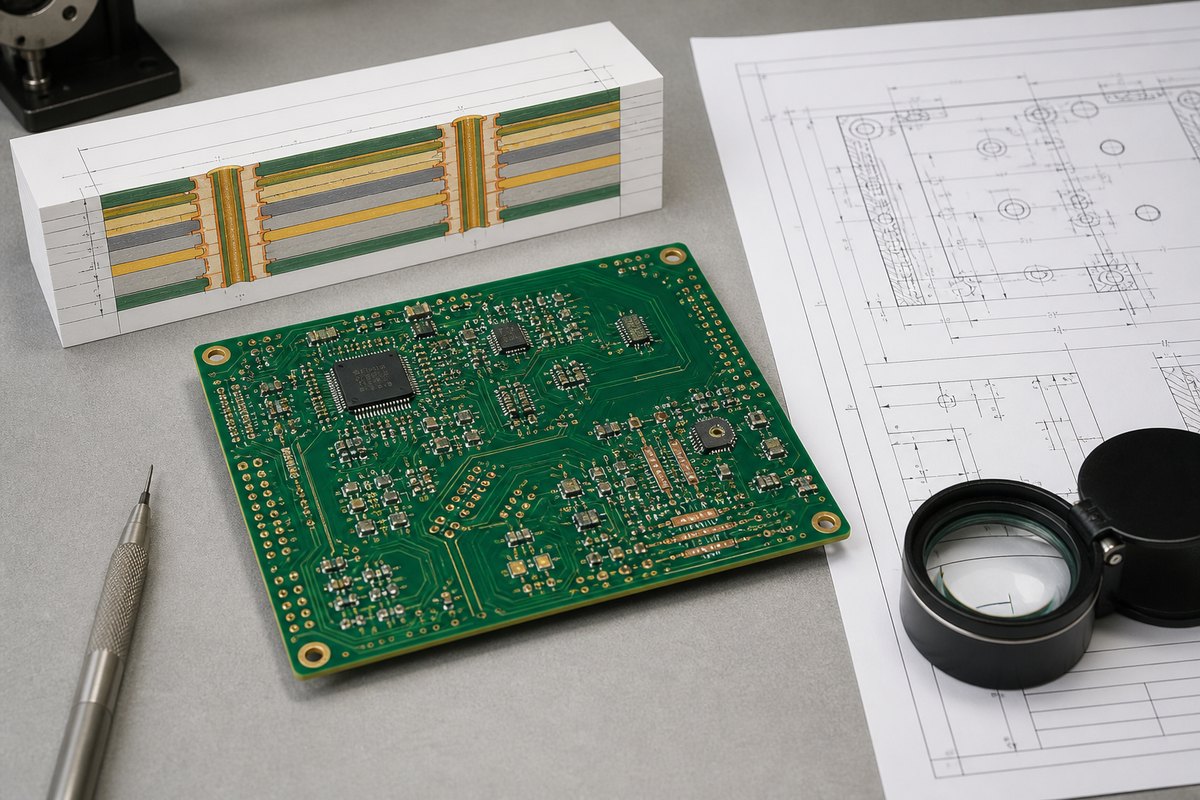
IPC-2222 defines the rigid-board details that sit beneath a generic PCB design. It touches electrical and thermal subjects, but it is not the sole source for current capacity, signal integrity, thermal analysis or every spacing rule. Those decisions may also draw on IPC-2221, product requirements and other applicable standards.
| Design Area | IPC-2222 Scope |
|---|---|
| Materials | Laminate, dielectric, conductive and embedded-component materials, including property and substitution controls |
| Board construction | Board type, dielectric arrangement, copper construction and overall thickness |
| Mechanical features | Finished profile, cutouts, notches, slots, routing, scoring, datums and tolerances |
| Assembly interface | Board and array features that affect component attachment, handling and separation |
| Holes and interconnections | PTHs, unsupported holes, vias, fit, tolerance, plating and aspect ratio |
| Lands and planes | Land geometry, annular copper, nonfunctional lands and plane interaction |
| Circuit features | Edge spacing, balanced conductors, offset lands and large conductive areas |
| Documentation | Controlled information needed to communicate the approved rigid-board design |
How Does IPC-2222 Guide PCB Material and Laminate Selection?
“FR-4” is not a complete material specification. An IPC-2222 review needs enough information to connect the laminate system, dielectric construction, copper and permitted substitutions with the board’s electrical, thermal and mechanical demands.
- Laminate system: name the approved material grade or define the properties and test methods that an equivalent material must satisfy. A glass transition temperature value alone does not define the full material behavior.
- Core and prepreg: show the layer sequence and target dielectric thicknesses. The design and fabrication teams should agree which dielectric separates each copper layer and reference plane.
- Copper construction: distinguish starting foil from finished copper where plating changes the result. Copper thickness affects etching, spacing, current paths, thermal behavior and impedance geometry.
- Material properties: review the electrical, thermal, moisture and mechanical properties that affect the application instead of selecting a laminate from one headline value.
- Substitution control: state which changes require engineering approval. A substitute that changes dielectric, thermal-expansion or pressed-thickness behavior can invalidate an otherwise completed review.
This is a material-definition exercise, not a full stackup tutorial. The review succeeds when the proposed construction can be checked without guessing which laminate, dielectric or copper assumptions were used.
What Does IPC-2222 Require for PCB Thickness, Profiles and Mechanical Features?
Mechanical fit depends on the finished board, not the nominal CAD model. Finished thickness, the delivered profile and functional datums must still fit the connector, enclosure, guide rail or mounting system at their tolerance limits.
- Finished thickness: state a nominal value and the applicable overall tolerance. Compare the complete delivered range with card-edge connectors, guides, press-fit tooling and enclosure slots.
- Board profile: provide closed, unambiguous outline geometry and identify the dimensions that control the finished edge.
- Cutouts, slots and notches: define finished size, position, corner radius and plated status where relevant. Check the geometry against mating hardware and router capability.
- Mechanical datums: locate mounting holes, connectors and critical features from shared datums. Temporary panel rails should not control the dimensions of the delivered board.
- Tolerance purpose: tighten only the dimensions that protect an actual interface. Unnecessary tolerance reduction can lower yield without improving product function.
How Does IPC-2222 Address Panelization, Routing and V-Scoring?
Routing, scoring and breakaway features define both the finished edge and the stress applied during depanelization. That is why they belong in the rigid-board design review. The IPC-2222B public contents specifically name scoring parameters, V-groove conductor clearance, low-stress breakaway tabs, mouse bites, routed slots and a break line.
- Panel borders: define rails, tooling features and the relationship between the array and the delivered boards.
- Routing: show routed outlines, internal channels and slots with the finished dimensions and process tolerances that matter to the board.
- V-scoring: agree the score geometry, residual web and conductor clearance with the fabricator. The score path and separation method should not be inferred from a line on an assembly drawing.
- Breakaway tabs and mouse bites: place them where separation will not load fragile components or leave an unacceptable edge.
- Copper and component clearance: evaluate the worst-case remaining distance after routing or scoring variation, not only the nominal CAD distance.
The PCB panelization guidelines cover assembly-side choices in more detail. If a tab, rail, score or routed channel changes, review it again; the change can affect handling, separation stress and the delivered edge.
What Does IPC-2222 Require for PTHs, NPTHs and Vias?
Start with what the hole does, then define its finished condition. Drill-tool size, finished-hole size, plating, tolerance, aspect ratio and component fit belong to one tolerance chain. Copying those values separately from another board can produce a combination that no longer fits or plates as intended.
- Plated-through hole: define the finished hole and compare its minimum size with the maximum component-lead envelope. Confirm that the remaining clearance supports insertion and the intended soldering process.
- Via: select the drill and finished geometry with the plated depth, board thickness, land size, registration and the fabricator’s process capability.
- Unsupported or non-plated hole: identify the hole as non-plated, state its finished size and tolerance, and review nearby copper and hardware contact.
- Press-fit hole: use the connector manufacturer’s finished-hole, plating, insertion and qualification requirements. An ordinary soldered-hole fit cannot define a press-fit interface.
- Aspect ratio: evaluate plated depth relative to drill diameter with the proposed stackup and process. It is a manufacturing review input, not one universal target for every supplier.
Consider an illustrative round lead specified as 0.60 ± 0.02 mm and a finished plated hole of 0.78 ± 0.05 mm. These are example design inputs, not IPC-2222 minimum limits.
| Parameter | Minimum-Clearance Case | Maximum-Clearance Case | Review Check |
|---|---|---|---|
| Lead diameter | 0.62 mm maximum | 0.58 mm minimum | Include lead shape, plating, straightness and positional variation. |
| Finished hole | 0.73 mm minimum | 0.83 mm maximum | Confirm the drawing specifies finished size rather than drill-tool size. |
| Diametral clearance | 0.11 mm | 0.25 mm | Check insertion and soldering across the complete assembly tolerance chain. |
The minimum diametral clearance is 0.73 − 0.62 = 0.11 mm; the maximum is 0.83 − 0.58 = 0.25 mm. A square lead needs its maximum corner-to-corner envelope checked against the minimum hole. Multi-pin insertion also depends on lead position, hole position and straightness.
How Does IPC-2222 Address Lands, Annular Rings and Plane Clearance?
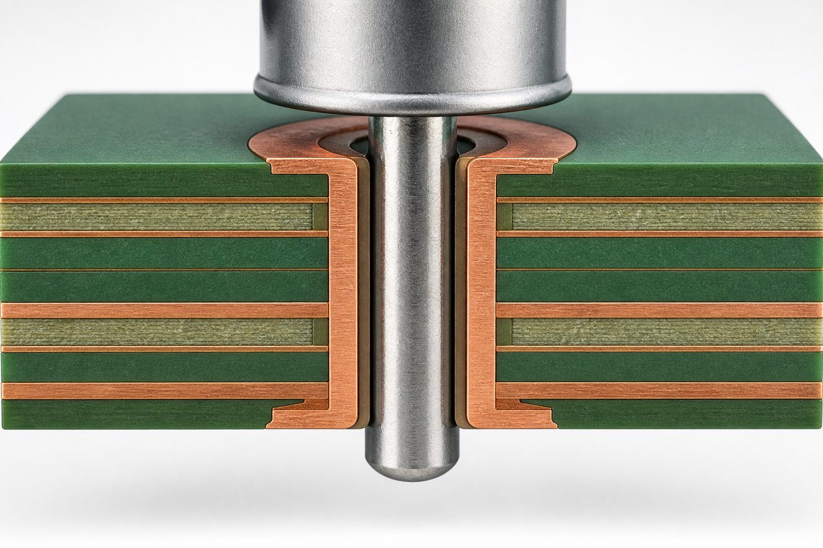
Hole size, land size, remaining annular copper and plane clearance have to be reviewed together. Increasing the land may protect the annular ring, yet reduce isolation to an unrelated plane. Treating either check alone hides that tradeoff.
- Start with hole function and finished size. The land must suit the plated or non-plated feature and the connection it is expected to make.
- Add fabrication allowance and registration. Drill position, layer registration, etching and finished-hole variation determine the copper that remains at the narrowest point.
- Evaluate the annular ring. The centered CAD difference between pad and hole diameters is only the nominal starting point.
- Recheck plane clearance. A larger land can improve remaining copper while reducing isolation to an unconnected plane.
- Choose the plane connection. Thermal relief or a solid connection should follow electrical duty, heat flow, copper thickness and soldering needs.
- Decide how to treat nonfunctional lands. Removal can affect registration support and clearance; retention can constrain routing and plane geometry.
The PCB annular ring guide develops this geometry further. Whenever a land changes, repeat the annular-ring, plane-clearance and conductor-spacing checks before closing the design.
What Does IPC-2222 Say About Conductor Features and PCB Edge Spacing?
Conductor geometry must survive both copper processing and edge formation. IPC-2222B specifically names printed board edge spacing, balanced conductors, offset lands and large conductive areas among its circuit-feature topics.
- Printed board edge spacing: measure from the finished routed or scored edge and include process tolerance. A nominal CAD clearance does not describe the minimum delivered distance.
- Balanced conductors: review copper distribution through the stack and across the panel. Strong asymmetry can contribute to distortion and should be discussed before release.
- Offset lands: use offset geometry only when the connection and fabrication allowances remain clear; do not treat it as a generic repair for congested routing.
- Large conductive areas: evaluate their electrical and thermal role together with copper balance, etching and assembly heat flow.
- Edge-process interaction: repeat the spacing check after changing routing, V-scoring, tabs, mouse bites or the board datum that defines the final profile.
What Changed from IPC-2222A to IPC-2222B?
IPC-2222B supersedes IPC-2222A and reorganizes several material, mechanical, interconnection and circuit-feature topics. The public previews for IPC-2222A and IPC-2222B reveal headings and table titles, not every requirement or numerical change. The comparison below is therefore a review guide rather than a clause-by-clause redline.
| Design Area | IPC-2222A | IPC-2222B | B-Revision Review |
|---|---|---|---|
| Material properties | Table 4-1 focuses on clad-laminate UL maximum operating temperatures. | Section 4.3.1 is “UL Parameters,” and Table 4-1 covers typical thermal properties of selected dielectrics. | Review the complete material property set and its test methods rather than carrying forward one temperature value. |
| Embedded component materials | No standalone embedded-component-materials section appears in the A preview contents. | Section 4.5 is “Electronic (Embedded) Component Materials.” | Identify the additional construction controls when components or materials are embedded. |
| Assembly array | Section 5.3.1 is “Assembly, Palletization and Test.” | Section 5.3.1 is “Assembly Array (or Pallet).” | Review the controlled array, rails, tooling features and separation method. |
| Overall thickness | Table 5-3 is “Printed Board Thickness Tolerance Levels.” | Table 5-3 is “Printed Board Overall Thickness Tolerance Levels.” | Confirm the delivered overall range required by connectors and mechanical interfaces. |
| Interconnection lands | The A preview proceeds to pad-to-plane clearance without a separate fabrication-allowance table. | Table 9-1 is “Minimum Standard Fabrication Allowance for Interconnection Lands.” | Recheck land geometry with process allowance before approving annular-ring or plane-clearance changes. |
| Plated-hole data | The preview lists PTH aspect-ratio and minimum diameter-tolerance tables. | The preview lists plated-hole aspect ratio, LMC/MMC hole-size limits and a recommended minimum drill-size table. | Revalidate drill, finished-hole limits, plating, aspect ratio and component fit as one chain. |
| Breakaway and edge features | The preview lists low-stress breakaway tabs and routed slots. | The figure titles explicitly include mouse bites, routed slots and a break line; the contents also name printed board edge spacing. | Recheck tabs, scoring, routing and minimum delivered copper-to-edge distance. |
Use the authorized editions before applying clause values or making a compliance claim. When a project moves from A to B, record the revision decision and update every affected design and procurement document.
How Should IPC-2222 Be Applied During PCB Design and DFM Review?
A practical review moves from board identity to controlled production data. DFM then tests the proposed design against a manufacturing process. It cannot choose the applicable standards, product requirements or approved exceptions on behalf of the project.
- Determine the board type. Identify the layer structure, blind or buried vias and any metal-core construction.
- Confirm the applicable IPC documents. Record the IPC-2221 and IPC-2222 revisions, performance basis and any customer-specific requirements.
- Define materials and construction. Approve the laminate system, dielectric sequence, copper build, finished thickness and impedance information.
- Review mechanical dimensions. Check the delivered profile, datums, cutouts, slots and component or enclosure interfaces at tolerance extremes.
- Check holes and lands. Separate PTH, via, press-fit and NPTH requirements; then review finished size, fit, aspect ratio, registration and annular copper.
- Check plane and edge clearance. Evaluate the complete tolerated hole-and-land feature and the minimum copper distance after the edge process.
- Review panel features. Confirm routing, scoring, tabs, mouse bites, rails, handling and separation effects.
- Release controlled production data. Reopen the final outputs and verify that the fabrication data, drill files, stackup and drawing describe the same revision.
What Files and Documentation Are Needed for an IPC-2222-Based PCB Design?
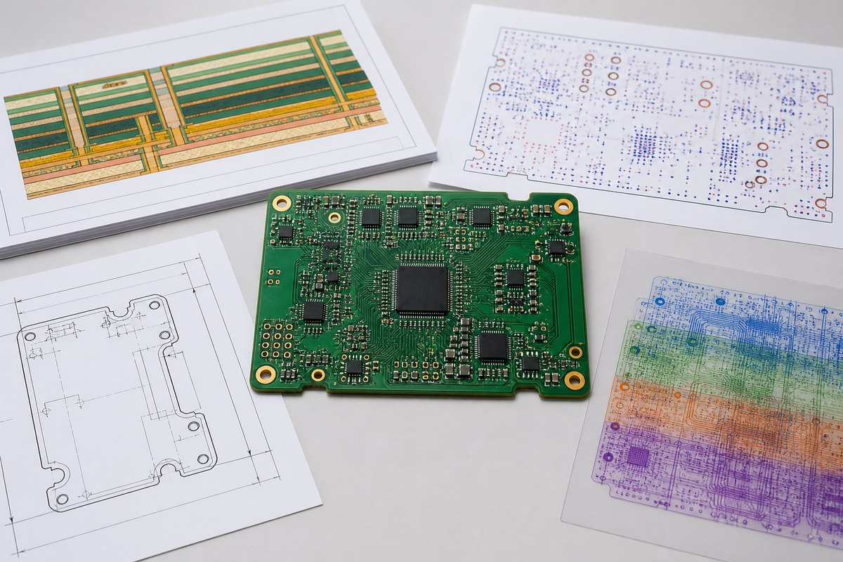
The released files must describe one approved board construction without contradiction. IPC-2222 does not prescribe a universal upload package, so the exact records depend on the product, contract and manufacturing route.
- Gerber, ODB++ files or another agreed fabrication format: copper, mask, legend, profile and other released layers.
- NC drill and rout data: plated and non-plated holes, slots, routed channels and any controlled-depth features.
- Fabrication drawing: board revision, dimensions, datums, tolerances, surface finish, scoring or routing and applicable standards with revisions.
- Stackup: material, dielectric construction, copper build, finished thickness and impedance information.
- Hole table: hole functions, finished sizes, tolerances, plated status and special press-fit or component requirements.
- Special requirements: approved substitutions, coupons, reports, inspection, test and any agreed exceptions.
After accepting a DFM change, update every file it touches. An approval email is not enough if the released drill table, stackup or drawing still carries the old value.
What Are the Most Common IPC-2222 Design Mistakes?
Most IPC-2222 mistakes begin with a wrong assumption about scope or with a nominal value taken out of its tolerance chain. Both can pass a superficial checklist while leaving the board definition incomplete.
- Treating IPC-2222 as a standalone standard: use it with IPC-2221 and the applicable performance, procurement and acceptance documents.
- Confusing PCB type with performance class: Type 3 describes a multilayer construction; it does not automatically mean Class 3.
- Specifying only nominal board thickness: include the finished tolerance and test the complete range against mechanical interfaces.
- Confusing drill size with finished-hole size: plating and process compensation separate the tool diameter from the delivered opening.
- Increasing land size without rechecking plane clearance: more annular copper can reduce isolation to unconnected copper.
- Ignoring the edge process: routing and scoring tolerances determine the minimum delivered copper-to-edge distance and separation stress.
- Using an outdated revision reference: identify the contractual revision and formally review any move from IPC-2222A to IPC-2222B.
- Treating DFM approval as automatic IPC compliance: DFM confirms selected manufacturing conditions; it does not choose every applicable standard or product requirement for the designer.
How Can EBest Circuit Support Rigid PCB Design and Manufacturing?
EBest Circuit can check whether the proposed rigid-board construction is buildable and whether the released files agree. The free DFM review supports prototype and production preparation, while standards selection, product qualification and compliance responsibility remain with the customer and project owners.
- Materials and stackup: review the proposed laminate system, copper build, finished thickness, impedance targets and substitution boundaries.
- Holes and lands: compare finished-hole intent, aspect ratio, annular copper, plane clearance and special connector requirements with the proposed process.
- Board edge and panelization: review routing, cutouts, V-scoring, tabs, rails and copper or component clearances.
- CAM and document consistency: compare Gerber or ODB++, NC drill, stackup and fabrication drawing for revision, outline, hole and construction conflicts.
- Prototype to production: keep approved DFM changes in the controlled files used for the prototype, follow-up builds and inspection plan.
Send your Gerber or ODB++ files, drill files, stackup and fabrication drawing to sales@bestpcbs.com for rigid PCB DFM review and quotation.
FAQs About IPC-2222
Q1: Is IPC-2222B the latest revision of IPC-2222?
A1: Yes, according to the IPC revision table checked on September 1, 2026. It lists IPC-2222B with an October 2020 date. Check the table again at project start and follow the revision named by the contract.
Q2: Where can I get the official IPC-2222 standard or IPC-2222B PDF?
A2: IPC provides a four-page preview that confirms the document identity, scope and contents. The preview is not the full standard, so use an authorized edition before applying clause values. Download the official IPC-2222B PDF preview (4 pages).
Q3: Can IPC-2222 be used without IPC-2221?
A3: No. IPC-2222 adds rigid-board-specific design requirements to the generic framework in IPC-2221.
Q4: Does a Type 3 board mean a Class 3 board?
A4: No. Type describes board construction; class describes performance expectations under the applicable documents.
Q5: Does IPC-2222 cover metal-core rigid PCBs?
A5: Yes. Types 5 and 6 are multilayer metal-core constructions. The project still has to define the material system, isolation, thermal conditions and supplier agreements.
Q6: Does IPC-2222 contain every electrical and thermal PCB design rule?
A6: No. IPC-2222 includes rigid-board electrical and thermal topics, but current capacity, signal integrity and detailed thermal analysis may also depend on IPC-2221, other standards and the product specification.
Q7: Are press-fit holes designed like ordinary soldered PTHs?
A7: No. Use the connector manufacturer’s finished-hole, plating, insertion and qualification requirements.
Q8: Does a fabricator’s DFM approval prove IPC compliance?
A8: No. DFM can confirm that selected features suit a manufacturing process. Compliance also depends on the chosen standards and revisions, the product requirements and any documented exceptions.
Q9: Should flex, rigid-flex or HDI boards use only IPC-2222?
A9: No. IPC identifies IPC-2223 for flexible and rigid-flexible applications and IPC-2226 for HDI printed boards. Use the standards that match the actual technologies in the design.
Q10: Which files should be sent first for an IPC-2222-based review?
A10: Send the current Gerber or ODB++, NC drill data, stackup and fabrication drawing first. Include any component or mechanical requirement that controls hole fit, finished thickness or the board edge.
You may also like





Tags: IPC-2222, PCB Design Standards, PCB DFM, rigid PCB design