A UBB PCB is the large, high-speed Universal Baseboard that connects multiple AI accelerator modules. For AI accelerators, its signal paths, power distribution, connector accuracy, and mechanical fit directly affect whether the system can be assembled and operated reliably. Even if a board passes a basic open/short test, incorrect impedance, voltage drop, connector alignment, or flatness can still cause unstable links, poor contact, overheating, or tray interference.
EBest Circuit (Best Technology) supports complex multilayer and HDI PCB manufacturability review, controlled-impedance fabrication, agreed sourcing and PCBA, inspection, and test coordination from prototype through production. System architecture and final platform validation remain with the customer. Planning a UBB PCB build? Send your stackup, fabrication data, drawings, impedance requirements, quantity, and assembly scope to sales@bestpcbs.com for an engineering and quotation review.
What Is a UBB PCB?
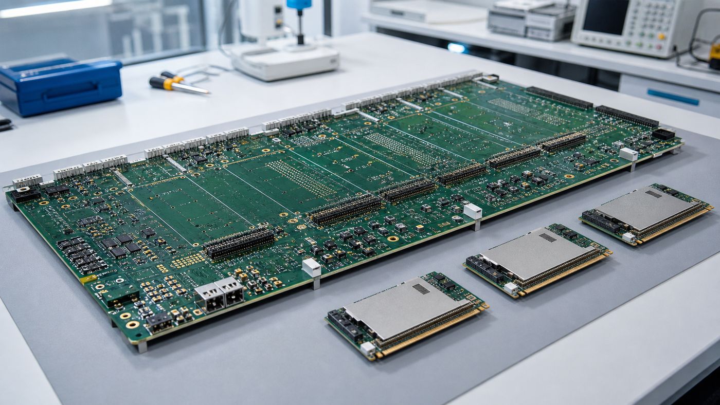
A UBB PCB is the Universal Baseboard that carries and connects multiple OAM accelerator modules in an AI computing platform. It acts as the common electrical and mechanical foundation between the accelerator modules and the rest of the system.
Its main roles include:
- Module connection: provides defined locations and interfaces for OAM modules.
- High-speed interconnect: carries host and module-to-module data paths.
- Power distribution: delivers the required power domains to accelerator modules and supporting circuits.
- Management support: routes clock, reset, monitoring, debug, and other sideband signals.
- Mechanical integration: aligns the modules with the host interface, power hardware, tray, and cooling system.
The UBB is not the accelerator module itself. The OAM carries the accelerator device and local circuitry; the UBB connects several modules into one platform. The applicable OCP/OAI revision and final production files determine the actual implementation.
How Does a UBB PCB Connect OAM Modules?
A UBB PCB connects OAM modules through precisely located high-density interfaces. In simple terms, the relationship is: OAM modules → UBB PCB → host, power, and management interfaces. Reliable operation also depends on mechanical compatibility with the tray and cooling hardware.
Four interfaces must agree:
- OAM-to-UBB: connector footprint, pad geometry, mating height, keep-outs, and module position.
- UBB-to-host: host-interface lanes, clocks, resets, and other control signals.
- UBB-to-power system: power connector locations, voltage domains, current paths, and standby rails.
- UBB-to-chassis: board outline, mounting holes, tray features, cooling clearance, and service access.
A connector can be electrically correct but mechanically unusable if hole locations, flatness, or mating clearance drift. Before fabrication, confirm the OAM, host interface board, power distribution board, tray, and cooling drawings use the same controlled revision.
What Are the Key UBB PCB Specifications?
A UBB PCB does not have one universal layer count, thickness, material, or copper construction. However, UBB designs usually share several manufacturing characteristics because they must connect multiple OAM modules on one large electrical and mechanical platform.
| Typical characteristic | Why it matters on a UBB PCB |
|---|---|
| Large format | Fits multiple OAM, host, power, and mounting interfaces. |
| High layer count | Provides routing, reference planes, and power layers. |
| Low-loss construction | Supports long accelerator signal paths. |
| Controlled impedance | Preserves critical signal geometry. |
| Complex vias/backdrill | Enables dense routing and limits via stubs. |
| High-current copper | Carries module power through planes and vias. |
| Mechanical control | Maintains flatness, alignment, and module fit. |
These are common UBB PCB characteristics, not fixed values. The released platform specification and fabrication package must define the actual board outline, finished thickness, layer construction, materials, copper weights, impedance targets, via structures, backdrill limits, connector requirements, and flatness tolerances.
Why Is UBB PCB Manufacturing So Challenging?
UBB PCB manufacturing is challenging because one large baseboard must support several OAM interfaces, long high-speed channels, high-current structures, and strict module-to-tray alignment at the same time. Each requirement is demanding on its own; their interaction on the same board creates the distinctive UBB manufacturing risk.
The main manufacturing risks are:
- Multiple OAM interfaces: connector fields must remain aligned with every module position across a large board.
- Long high-speed channels: material behavior, impedance geometry, vias, and backdrill accuracy accumulate across extended routes.
- High-current and fine-signal features: heavy power copper and precise signal geometry need compatible lamination, imaging, etching, and plating controls.
- Large-board flatness: copper imbalance or material movement can affect module seating, connector engagement, and tray installation.
- Late-stage yield exposure: a hidden lamination, plating, registration, or dimensional defect can scrap the complete multi-module baseboard.
The key difficulty is therefore not simply making a high-layer-count PCB. It is keeping signal, power, and mechanical requirements within tolerance across the entire UBB after repeated lamination, drilling, plating, and thermal processes.
What Stackup and Materials Are Used for UBB PCBs?
A UBB stackup normally has to satisfy three competing requirements: low-loss signal transmission, high-current power distribution, and dimensional stability across a large board. This is why UBB material selection cannot be separated from layer construction, copper balance, via design, and finished thickness.
A practical UBB stackup usually combines:
- High-speed signal layers: low-loss laminate, controlled dielectric thickness, suitable copper profile, and adjacent reference planes support long accelerator interconnects.
- Power and ground layers: multiple plane layers and appropriate copper weights distribute module current while providing stable signal return paths.
- Routing and transition structures: through vias, blind or buried vias, via-in-pad, and backdrilling may be combined where OAM escape density or stub control requires them.
- Balanced construction: symmetric materials and copper distribution help control bow, twist, thickness, and connector coplanarity on the large baseboard.
Low-loss materials are important because UBB channels can cross a substantial portion of the baseboard and pass through several via or connector transitions. These low-loss materials must also remain compatible with the selected copper, lamination cycle, and mechanical requirements. Heavy copper helps power delivery but can make etching, resin filling, lamination, and warpage control more difficult. The approved production stackup must balance both needs rather than optimizing either one in isolation.
A material brand alone does not define performance. The production stackup should state the actual dielectric system, glass style, copper profile, dielectric thickness, copper weights, impedance geometry, and permitted material alternatives.
How Does a UBB PCB Handle High-Speed Signals?
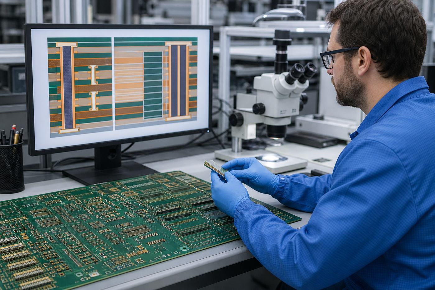
A UBB PCB handles high-speed signals by preserving controlled geometry and reference-plane continuity across long routes between multiple module and system interfaces. Because a UBB can combine extended traces with several via and connector transitions, small manufacturing deviations can accumulate into greater channel discontinuity or loss. Manufacturing must therefore reproduce the customer's validated materials, traces, vias, antipads, and residual stubs.
Evidence to request from the PCB manufacturer includes:
- An approved production stackup with the actual impedance geometry.
- Controlled differential-pair width, spacing, copper compensation, and reference planes.
- Backdrill depth and residual-stub control where required by the channel design.
- Registration checks for connector pads, vias, antipads, and plane clearances.
- Lot-linked impedance coupons and TDR (time-domain reflectometry) results.
TDR confirms the manufactured impedance structure; it does not prove the complete system channel. The customer validates signal integrity, while the manufacturer provides fabrication records that can be compared with simulation and platform results.
How Does a UBB PCB Handle High-Power Distribution?
A UBB PCB handles high-power distribution by reproducing the customer's defined power paths through power connectors or press-fit interfaces, copper planes, neck-down regions, plated vias, and via arrays. The fabrication task is to preserve the specified copper cross-section and geometry from each power entry to the relevant module interfaces.
The most important PCB manufacturing features are:
- Copper construction: specified foil and plated copper thickness must be achieved on planes, traces, and finished holes.
- Plane and neck-down geometry: local restrictions near connectors, cutouts, or dense signal regions must not reduce the intended current path.
- Via arrays: finished hole size, plating thickness, via count, and spacing determine the available vertical copper cross-section.
- Power connector holes: drilled diameter, plating, positional tolerance, and press-fit requirements must match the released connector drawing.
- Heavy-copper lamination: resin filling, copper balance, and material flow must be controlled to avoid voids, thickness variation, and warpage.
These features influence resistance, voltage drop, temperature rise, and mechanical reliability, but the manufacturer does not replace the customer's power-integrity design. EBest reviews whether the released copper, hole, plating, and material requirements are manufacturable and provides the agreed copper records, microsections, dimensional results, or electrical tests for acceptance.
How Should a UBB PCB Be Inspected and Tested?
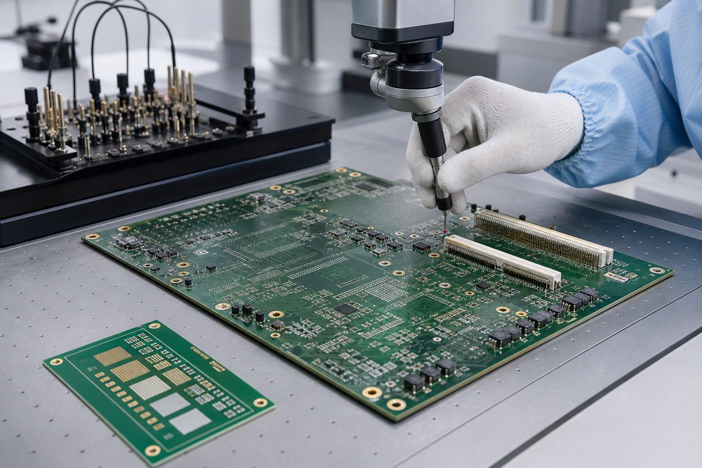
A UBB PCB should be inspected with a risk-based plan that covers internal circuitry, vias, impedance, dimensions, mechanical fit, and—when assembly is included—hidden solder joints and customer-defined functional checks.
Ask for evidence that answers these customer questions:
- Was the approved material and stackup used? Review material and stackup records.
- Were circuit defects detected before lamination or shipment? Review internal and external AOI results.
- Will the board fit the modules and tray? Check the outline, connectors, mounting holes, thickness, and flatness report.
- Are hidden vias and backdrills acceptable? Review microsections for plating, resin fill, lamination, and residual stubs.
- Does the bare board match the netlist? Require 100% continuity and isolation testing.
- Was controlled impedance achieved? Review lot-linked TDR coupon results.
- Are hidden assembly joints acceptable? Use AOI or X-ray where the PCBA risk requires it.
- Does the assembled board meet the agreed function? Use customer-defined fixtures and pass/fail limits.
Decide before ordering which records are required for prototypes and which must accompany every production lot. EBest can coordinate the required inspection records and keep them tied to the correct lot and file revision.
How to Choose a UBB PCB Manufacturer?
Choose a UBB PCB manufacturer by checking whether its real process capability, engineering response, verification evidence, and production controls match your released board—not by accepting a generic multilayer-PCB claim.
Ask four customer-focused questions:
- Can they build it? Match board size, thickness, materials, HDI/via construction, backdrill, impedance, and power features.
- Can they explain the risks before quoting? Expect clear questions about stackup, drill pairs, copper balance, tolerances, and substitutions.
- Can they prove what they inspected? Define electrical test, TDR, microsections, dimensions, AOI/X-ray, and lot records.
- Can they repeat the process in production? Confirm material continuity, revision control, critical processes, and production inspection.
A representative sourcing problem occurs when a large UBB is quoted only by layer count and quantity. If material construction, board size, backdrill, impedance reporting, and flatness are clarified after the order, the price, lead time, or yield expectation can change. A better supplier resolves these items before the build and records every approved exception.
EBest Circuit can review controlled fabrication data, stackup, drill files, drawings, impedance requirements, quantities, and the agreed PCBA/test scope. Our role is to identify manufacturing gaps early, build to the approved package, and provide the agreed evidence for customer acceptance.
FAQs About UBB PCB
Is a UBB PCB the same as an OAM module?
No. The UBB is the shared baseboard that connects multiple OAM modules. An OAM is the accelerator module installed into the UBB interface.
Does every UBB PCB use the same layer count and material?
No. Stackup, materials, copper, vias, and thickness depend on the platform's signal, power, mechanical, and manufacturing requirements.
Does an OCP UBB specification replace the production files?
No. It provides an architecture and interface reference. Manufacturing still requires final fabrication data, drawings, stackup, drill files, materials, and acceptance criteria.
What should be tested before a UBB PCB is assembled?
Confirm the stackup, dimensions, continuity, isolation, critical vias, impedance, flatness, and connector locations before assembly.
What files should I send for a UBB PCB quotation?
Send the fabrication data, drill files, approved or target stackup, impedance requirements, material notes, mechanical drawings, acceptance criteria, revision, quantities, and—if needed—BOM, placement, assembly, and test files.
Need a UBB PCB manufacturing review? Send your final files, quantities, and PCB/PCBA requirements to sales@bestpcbs.com. EBest Circuit will identify open manufacturing questions and confirm the next steps before production.
You may also like






Tags: AI Server PCB, UBB PCB, Universal Baseboard