





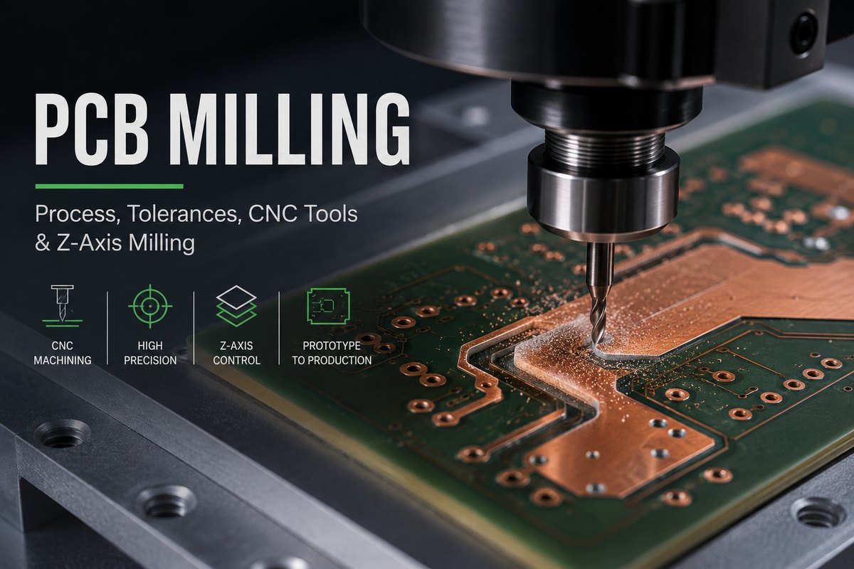
PCB milling means using a rotating cutting tool to remove copper, laminate, or both from a printed circuit board. The term usually describes two different processes:
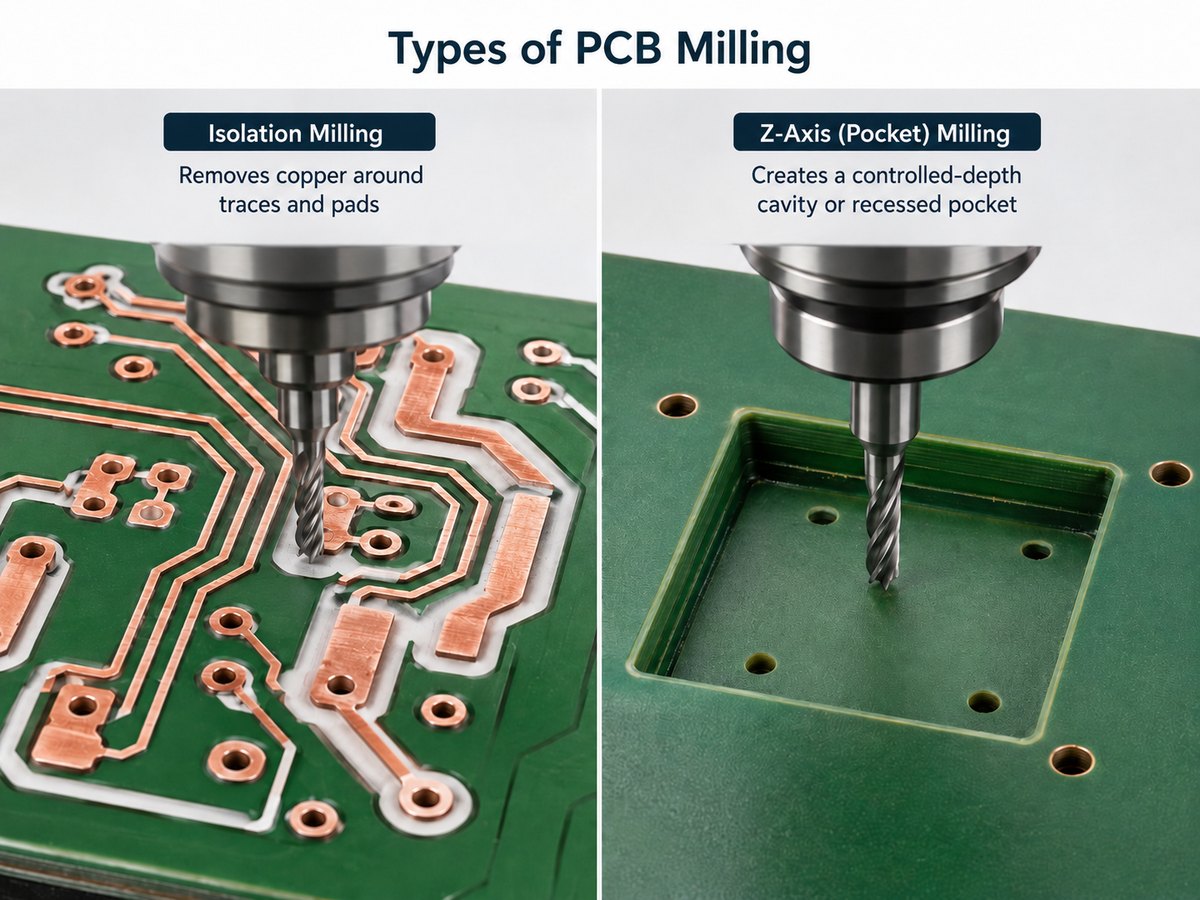
- Isolation milling: removing copper around traces and pads to make a prototype PCB.
- Controlled-depth milling: removing part of the PCB thickness to form cavities, pockets, steps, or recessed areas.
The distinction matters. A desktop CNC machine used for a quick prototype has very different design limits from a production PCB that requires a controlled-depth cavity above an internal copper layer.
This guide explains both applications and focuses on the practical questions engineers and buyers need to answer before choosing the process or requesting a quote.
What Is PCB Milling?
PCB milling is a subtractive manufacturing process. Instead of building a feature by adding material, a cutter removes unwanted material from the board.
For prototype boards, milling normally removes copper to create electrical isolation between traces. The same machine may also drill holes and route the final outline.
In PCB manufacturing, milling is also used for mechanical structures such as:
- Cavities and pockets
- Recessed connector areas
- Local thickness reduction
- Internal slots
- Edge steps
- Component clearance areas
Standard PCB routing normally cuts through the full board thickness. Controlled-depth milling stops at a defined Z position and leaves a specified amount of material behind.
That difference becomes especially important on multilayer boards, where the milled feature may sit close to an internal copper layer.
What Are the Main Types of PCB Milling?
The two main categories are isolation milling and controlled-depth milling.
PCB Isolation Milling
PCB isolation milling removes narrow strips of copper around traces and pads. The remaining copper forms the circuit.
It is mainly used for:
- Same-day prototypes
- Simple single- or double-sided circuits
- Test fixtures
- University and laboratory work
- RF test structures
- Early proof-of-concept boards
Its main limitation is feature density. As traces and gaps become smaller, tool diameter, spindle runout, board flatness, and Z-axis accuracy become much more critical.
Controlled-Depth and Z-Axis Milling
Controlled-depth milling removes laminate to a specified depth without cutting through the entire PCB.
Typical applications include:
- Recessed components
- Low-profile connectors
- Mechanical enclosure clearance
- Local board thinning
- RF structures
- Pockets for thermal or mechanical interfaces
On a multilayer PCB, the milling depth has to be checked against the real stackup. A cavity that is too deep can expose copper, reduce dielectric spacing, or weaken the board.
How Does the PCB Milling Process Work?
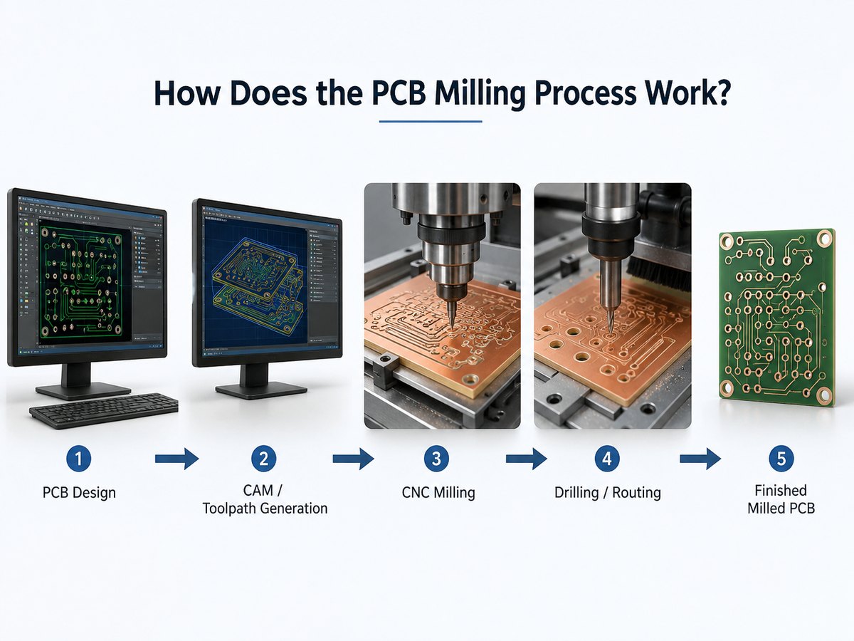
The workflow varies slightly between prototype milling and production milling, but the basic process is similar:
- Prepare the design files. Copper, drill, outline, and milling data must be clearly defined.
- Generate the CNC toolpath. CAM software converts the design into machine movements.
- Secure the board. Poor workholding can introduce height variation or movement.
- Set the Z reference. The machine establishes the PCB surface or another defined datum.
- Mill the required areas.
- Drill holes and route the outline if needed.
- Inspect dimensions and remaining thickness.
For isolation milling, surface probing is often valuable because even a slightly warped PCB can change the cutting width of a V-bit.
For controlled-depth milling, the more important question is often not simply “How deep should the tool cut?” but:
How much PCB thickness must remain after milling?
For a critical recess, defining the remaining thickness usually gives the manufacturer a clearer inspection target.
What Equipment Is Used for CNC PCB Milling?
A useful PCB milling machine needs more than basic CNC movement. The result depends on several machine characteristics.
Key factors include:
- Spindle runout: excessive runout increases the effective cutting width.
- X-Y positioning: affects trace geometry, slots, holes, and cavity dimensions.
- Z-axis repeatability: critical for both isolation width and cavity depth.
- Surface probing: compensates for board-height variation.
- Workholding: the PCB must remain flat without being bent by clamps.
- Dust extraction: FR4 milling creates fiberglass and resin dust that should be collected properly.
Desktop PCB milling machines are mainly used for rapid prototyping. PCB factories typically use dedicated CNC routing or controlled-depth equipment for production boards.
A machine with a fine positioning specification does not automatically guarantee equally fine PCB features. Cutter condition, tool runout, board flatness, and process setup still affect the result.
Which PCB Milling Bits and Tools Should You Use?
Tool choice should follow the feature being machined, not simply the PCB material.
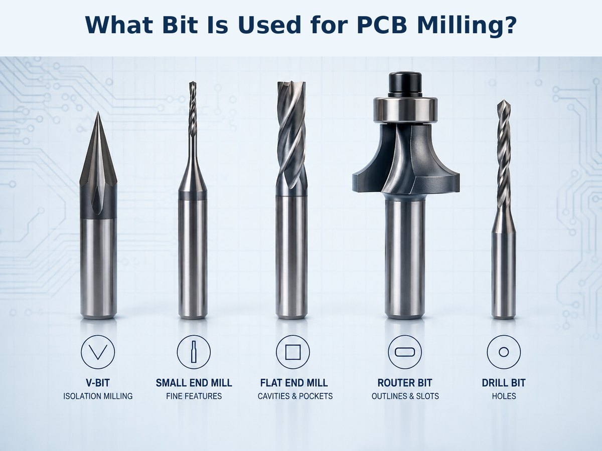
| Tool | Typical Use | Main Limitation |
|---|---|---|
| V-bit | Copper isolation | Cut width changes with depth |
| Small end mill | Fine slots and isolation | Small tools break easily |
| Flat end mill | Cavities and pockets | Internal corners remain rounded |
| Router bit | Outline and larger slots | Diameter limits corner radius |
| Drill bit | Through holes | Runout affects finished hole size |
V-bits are common for prototype isolation milling because they can produce narrow cuts. Their weakness is that cutting width changes as the tool moves deeper into the board.
Small end mills produce a more predictable width, but they are more fragile.
For cavity milling, cutter diameter also controls the minimum internal corner radius. If a component requires a square corner, the mechanical drawing may need a relief feature rather than an impossible zero-radius corner.
What Software and Files Are Needed for PCB Milling?
The normal PCB milling software and data flow is:
PCB CAD → CAM software → CNC toolpath → machine
For basic isolation milling, the fabrication package normally includes:
- Copper Gerber files
- NC drill files
- PCB outline
- Registration information for double-sided boards
Controlled-depth milling needs more detail. A useful production package should include:
- Mechanical or milling layer
- Dimensioned drawing
- Milling location
- Required depth or remaining thickness
- Depth tolerance
- Milling side
- Corner radius
- Stackup information where relevant
Avoid relying on notes such as “mill this area” when the geometry affects an internal layer or mechanical fit.
The drawing and Gerber data should also agree. Conflicting dimensions are one of the easiest ways to delay quotation or engineering approval.
What PCB Milling Tolerances and Design Rules Matter?
There is no single tolerance that describes every PCB milling feature.
A profile, a narrow slot, an isolation groove, and a controlled-depth cavity are produced differently and should be evaluated separately.
| Feature | Main Process Variable | Design Check |
|---|---|---|
| Isolation width | Tool geometry and Z depth | Do not design to the theoretical tool tip |
| Trace spacing | Cutter width and registration | Leave margin for process variation |
| Slot width | Tool diameter | Confirm tool access |
| Pocket depth | Z-axis control | Define the reference surface |
| Remaining thickness | PCB thickness + depth variation | Specify final required thickness |
| Internal corner | Cutter diameter | Allow a radius or relief |
| Copper-to-edge clearance | Routing and layer registration | Keep copper away from milled areas |
| Cavity-to-inner-layer spacing | Stackup and depth tolerance | Check actual dielectric thickness |
For commercial fabrication, published minimum capabilities should not automatically become design targets. Features are usually easier and more economical to manufacture when they sit comfortably inside the process window.
A cavity close to an internal plane is a good example. If the nominal remaining dielectric is only slightly larger than the combined PCB-thickness and milling tolerances, the design may need additional clearance.
Why Is Z-Axis Control Critical in PCB Milling?
Z-axis control affects both prototype accuracy and production reliability.
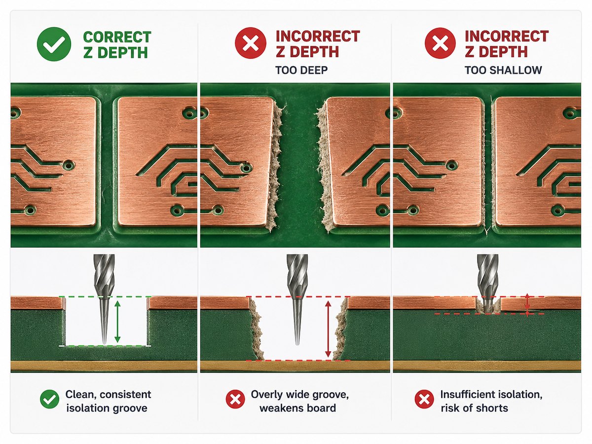
With a V-bit, a deeper cut creates a wider groove. If the PCB surface varies in height, one area may be cut too deeply while another is not fully isolated.
Possible results include:
- Inconsistent isolation width
- Reduced trace width
- Uncut copper bridges
- Excessive laminate removal
Surface probing helps compensate for this during desktop PCB milling.
Controlled-depth PCB milling has a different tolerance problem. The final remaining material is influenced by several variables:
PCB thickness variation + layer-position variation + milling-depth variation
If the remaining dielectric protects an internal conductor or provides voltage spacing, mechanical strength, or impedance control, that requirement should be stated on the fabrication drawing rather than left for the manufacturer to infer.
PCB Milling vs Etching: Which Is Better?
PCB milling is attractive when speed and in-house iteration matter. Conventional PCB fabrication is generally better when density, multilayer construction, plating, or production repeatability matter.
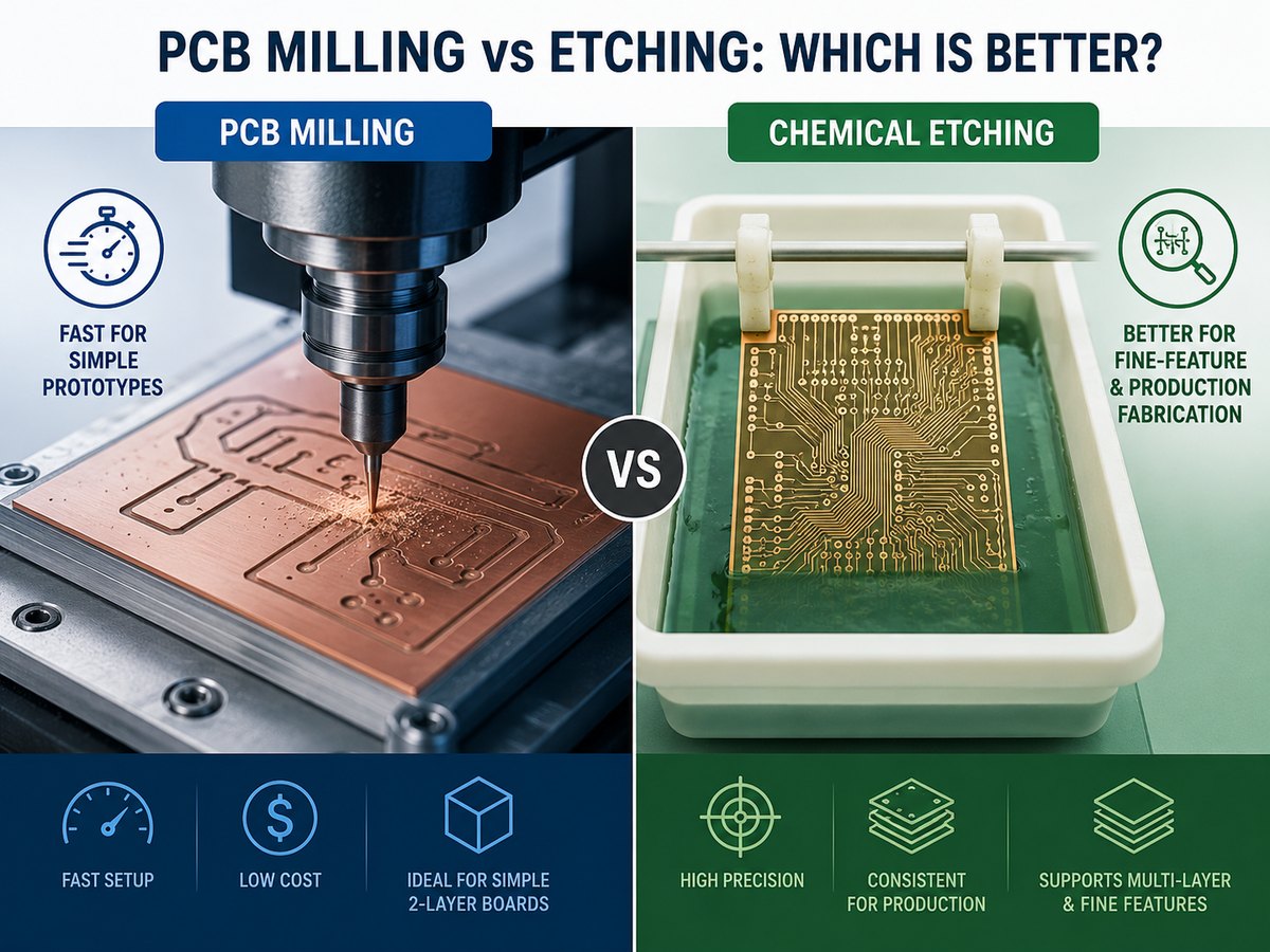
| Factor | PCB Milling | Conventional PCB Fabrication |
|---|---|---|
| Same-day in-house prototype | Strong advantage | Usually slower |
| Chemical copper patterning | Not required | Normally required |
| Fine traces and spacing | More limited | Better |
| BGA / HDI designs | Poor fit | Suitable |
| Multilayer boards | Limited | Standard process |
| Plated through holes | Extra process needed | Integrated |
| Design iteration | Very fast | Requires another build |
| Tool wear | Important | Not relevant to copper imaging |
| Production volume | Inefficient | Scalable |
| Controlled-depth cavities | Possible | Common in advanced fabrication |
A simple sensor board or RF experiment may be a good candidate for isolation milling. A multilayer board with fine-pitch BGA routing, plated vias, controlled impedance, and production surface finish is not.
When Should You Use PCB Milling for Prototypes?
PCB milling makes the most sense when the value comes from fast iteration rather than production-representative construction.
It works well for:
- Early electrical validation
- Simple analog and digital circuits
- RF geometry experiments
- Test fixtures
- Mechanical PCB trials
- Low-complexity one-off boards
Professional PCB fabrication is usually the better choice when the prototype requires:
- Fine-pitch BGA routing
- Microvias
- Multilayer registration
- Plated through holes
- Controlled impedance
- Production solder mask
- ENIG or another controlled finish
- Reflow or reliability testing
The better purchasing question is not simply, “Can this PCB be milled?”
“Will a milled board reproduce the conditions I actually need to validate?”
If the answer is no, saving a day on fabrication may create a prototype that tells you very little about the final product.
What Should You Specify When Ordering a PCB With Milling?
Controlled-depth milling should be treated as a defined mechanical feature, not a loose fabrication note.
For quotation, provide:
- Gerber or ODB++ data
- NC drill files
- PCB outline
- Stackup
- Finished board thickness
- Mechanical drawing
- Milling location and dimensions
- Required depth or remaining thickness
- Depth tolerance
- Milling side
- Minimum corner radius
- Copper restrictions near the milled area
- Prototype and production quantities
Instead of writing:
Mill pocket 0.8 mm deep.
A more useful definition is:
Mill from the top side and leave 0.80 ±0.10 mm board thickness in the indicated pocket.
That gives the manufacturer a measurable final condition.
For complex cavities, the stackup should be reviewed before production. At EBest Circuit, we can review cavity depth, internal copper clearance, remaining laminate thickness, and cutter access before the job is released.
Clear milling data also improves quotation accuracy because fewer assumptions have to be built into the price.
PCB Milling FAQs
What is PCB milling used for?
PCB milling is mainly used for rapid prototype circuits and mechanical PCB features such as pockets, cavities, slots, and local thickness reduction.
How accurate is PCB milling?
Accuracy depends on the feature. Cutter runout, PCB flatness, Z-axis control, board thickness, tool size, and machine positioning all contribute to the finished result.
For commercial designs, use the manufacturer’s tolerance for the specific feature rather than applying one general CNC tolerance to the whole PCB.
What bit is best for PCB milling?
V-bits are common for copper isolation. Small end mills are useful where a more consistent cutting width is needed. Flat end mills are usually preferred for cavities, while router bits are used for profiles and larger slots.
Can a CNC machine mill a PCB?
Yes. A suitable CNC machine can isolate traces, drill holes, route profiles, and machine cavities.
For fine PCB work, spindle runout, Z-axis accuracy, proper fixturing, and dust extraction matter as much as the nominal machine resolution.
What is PCB isolation milling?
PCB isolation milling mechanically removes copper around traces and pads so that the remaining copper forms the circuit. It is mainly used for simple and rapid prototypes.
What is Z-axis milling in PCB manufacturing?
Z-axis milling controls how deeply the cutter enters the PCB. It is used to keep isolation cuts consistent and to create production features such as controlled-depth cavities, recessed areas, and local board thinning.
Conclusion
PCB milling is useful in two very different situations: fast isolation milling for simple prototypes and controlled-depth machining for engineered PCB structures.
For prototype work, the main limits are feature size, tooling, board flatness, and Z-axis control. For manufactured boards, the more important issues are cavity geometry, remaining thickness, stackup, internal copper clearance, and tolerance.
If your PCB requires cavities, recessed areas, special slots, or controlled-depth milling, send the fabrication files and mechanical drawing to sales@bestpcbs.com for a manufacturability and quotation review.
You may also like








Tags: pcb milling, pcb milling bits, pcb milling machine, pcb milling process, pcb milling software