For an electronic components PCB project, choose parts by translating product requirements into electrical, thermal, mechanical, manufacturing, and supply-chain limits. The right part must perform its circuit function, fit a verified land pattern, survive the real environment, remain sourceable, and pass prototype and production validation. A part number is acceptable only when every one of those conditions is documented.
Do not begin by searching for the cheapest IC or the smallest package. Begin with a requirements sheet, select the main functional devices, derive their support circuits from current manufacturer documents, and then evaluate ratings, package constraints, availability, and verification evidence. The following sequence keeps component decisions connected to PCB layout and PCBA production instead of treating the BOM as a purchasing list created after design.
What Requirements Should You Define Before Choosing Electronic Components for PCB Design?
Define the operating envelope before selecting any manufacturer part number. A concise component requirements sheet should state what the circuit must do and the conditions under which it must do it. Without this baseline, a component can look suitable in a parametric search while failing on startup current, logic compatibility, enclosure temperature, lifetime, or assembly constraints.
| Requirement Area | Questions to Resolve | Component Decision Affected |
| Function and interfaces | What must be sensed, processed, switched, stored, driven, or communicated? | Main IC, analog front end, driver, memory, protection, and connector family |
| Power | What are the nominal, startup, transient, fault, and sleep conditions? | Regulators, MOSFETs, diodes, inductors, capacitors, fuses, and current-sense parts |
| Environment | What are the ambient temperature, humidity, vibration, contamination, and altitude limits? | Temperature grade, package, sealing, corrosion risk, creepage, and coating compatibility |
| Mechanical envelope | What are the board outline, height limits, connector positions, mounting loads, and service needs? | Package height, connector style, retention, heatsink, and keepout requirements |
| Production | What volume, assembly process, inspection method, and repair strategy will be used? | Package pitch, termination visibility, tape-and-reel option, moisture sensitivity, and test access |
| Compliance and lifetime | Which market, safety, substance, automotive, industrial, or customer requirements apply? | Qualification grade, declarations, traceability, lifecycle status, and approved sources |
Rank each requirement as mandatory, target, or optional. Also record the source of the value: system specification, interface standard, safety analysis, mechanical model, test requirement, or customer contract. This prevents a desirable feature from being mistaken for a release condition and gives reviewers a clear reason for accepting or rejecting a candidate.
How Do You Select the Main Electronic Components for the Required PCB Function?
Select the architecture first and the exact orderable device second. The main IC must cover the required function with enough processing, interfaces, analog performance, memory, protection, and power capability, but unused features add cost, power, routing difficulty, and software risk.
- Match the essential function: List required channels, resolution, bandwidth, timing, memory, communication interfaces, and control features before comparing product families.
- Check system compatibility: Confirm supply rails, input thresholds, output drive, clocking, startup state, reset behavior, and communication voltage levels.
- Assess implementation burden: Include firmware maturity, programming tools, reference software, external memory, calibration, and required analog support.
- Compare usable packages: A device available only in a package that cannot be routed, inspected, reworked, or thermally managed is not a practical choice.
- Evaluate failure behavior: Determine what happens during undervoltage, overcurrent, loss of communication, overheating, open sensors, and shorted loads.
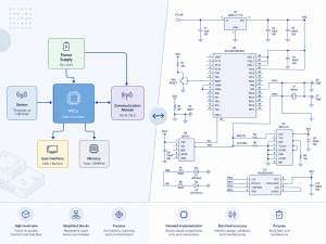
A functional block diagram is useful at this stage. Assign one owner component to each major block, then record the assumptions that connect the blocks. This exposes missing level translators, isolation, protection, clock sources, interface transceivers, and power rails before the schematic becomes difficult to change.
How Do Datasheets Define the Support Components Around a Main PCB Device?
Use the current datasheet, reference design, and application notes to build each support network. Do not copy only the typical application drawing: check the surrounding equations, operating conditions, layout notes, component tolerances, and package-specific requirements.
For a power converter, calculate the inductor, input and output capacitors, feedback network, compensation, diode or synchronous switch requirements, current sense, and thermal loss using the actual input range and load profile. For a processor, review every supply domain, decoupling group, reset and boot pins, crystal or clock network, programming interface, pull resistors, and unused-pin instructions. Manufacturer guidance may also make placement part of the electrical requirement; for example, high-frequency decoupling capacitors often need a very short connection to the pin and return path.
- Freeze the document revision: Record the datasheet revision, errata, application notes, package drawing, and reference design used for selection.
- Extract mandatory networks: Separate required components from optional performance-tuning or evaluation-board features.
- Recalculate for the application: Replace example voltages, currents, frequency, temperature, and load assumptions with project values.
- Transfer layout constraints: Add placement, loop-area, grounding, thermal-via, and routing requirements to the PCB design rules.
- Record validation items: Identify values that must be tuned or confirmed during prototype measurement.
Which Electrical Ratings and Tolerances Matter for PCB Component Selection?
Compare worst-case circuit stress with the component’s guaranteed operating limits, not just its headline rating. Absolute maximum ratings describe a damage boundary, not a recommended continuous operating point. Use the recommended operating range and verified application conditions for normal design.
| Component | Parameters to Check | Often-Missed Effect |
| Resistor | Resistance, tolerance, rated power, working voltage, pulse rating, TCR | A small resistor may meet average power but fail a startup or surge pulse |
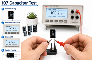
| MLCC | Capacitance, tolerance, voltage, dielectric, temperature range, ESR | Effective capacitance can fall under DC bias, temperature, and aging |
| Inductor | Inductance, tolerance, saturation current, RMS current, DCR, self-resonant frequency | Peak current can cause saturation before average-current heating becomes excessive |
| Diode | Reverse voltage, forward current, surge current, forward drop, leakage, recovery | Leakage and reverse recovery can dominate high-temperature or switching behavior |
| MOSFET | VDS, ID, RDS(on) at actual gate voltage, gate charge, SOA, thermal resistance | A headline current rating may assume a thermal condition unavailable on the real PCB |
| IC | Supply range, I/O limits, accuracy, timing, power, junction temperature | Electrical performance may be guaranteed over a narrower range than basic operation |
| Connector | Current per contact, voltage, contact resistance, cycles, wire size, temperature rise | Total current and adjacent loaded contacts can reduce usable current per pin |
Use worst-case analysis for tolerance stacks. A divider, filter, oscillator, current limit, feedback loop, and sensor channel can all fail even though every nominal value appears correct. For capacitors, use the manufacturer’s effective-capacitance data at applied voltage and temperature; a power-supply design that needs 10 µF cannot assume that a part marked 10 µF provides that value in circuit.
How Do Derating, Temperature, and Environment Affect Electronic Components?
Derating must follow the real stress mechanism and the component manufacturer’s conditions. A single blanket percentage is not valid for every resistor, capacitor, semiconductor, connector, or application. Establish maximum circuit stress, include tolerances and transients, calculate temperature rise, and then apply the project reliability policy.
Thermal analysis must connect the component package to the board. Power dissipation, copper area, thermal vias, airflow, neighboring heat sources, enclosure temperature, and duty cycle determine junction or hot-spot temperature. Manufacturer thermal parameters are tied to stated test boards and conditions; they are not universal package constants.
Environmental selection also covers humidity, condensation, corrosive gases, salt, vibration, shock, UV exposure, cleaning chemistry, and conformal-coating compatibility. Temperature grade alone does not prove that a device, termination finish, connector seal, or solder joint is suitable for the complete environment.
How Do PCB Component Packages, Footprints, Pinouts, and Assembly Processes Affect Selection?
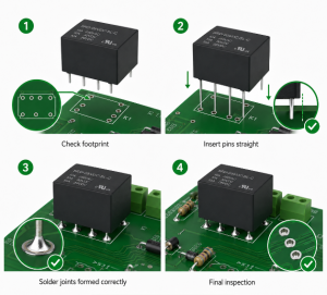
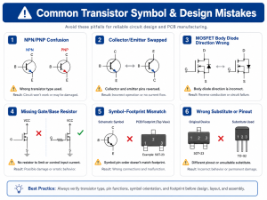
A component is not PCB-ready until its exact package code and land pattern have been verified together. Similar family names can hide differences in body size, pitch, exposed pad, pin numbering, lead finish, package height, or thermal behavior.
- Verify the package drawing: Match the orderable suffix to the manufacturer’s outline drawing, pin-one marker, terminal dimensions, pitch, coplanarity, and exposed-pad definition.
- Build the land pattern deliberately: Use manufacturer and applicable IPC guidance, then adapt solder-mask, paste, courtyard, and via rules to the assembler’s process capability.
- Check assembly access: Confirm pick-and-place packaging, nozzle access, component clearance, polarity visibility, AOI view, X-ray need, rework access, and hand-solder limitations.
- Review moisture handling: Record moisture-sensitivity and floor-life controls for packages that require dry storage or baking decisions.
- Test the library model: Compare symbol pins, footprint pads, 3D model, courtyard, and BOM package field against the same manufacturer document.
Fine-pitch and bottom-terminated packages can reduce area and electrical parasitics, but they increase stencil, voiding, X-ray, routing, and rework demands. NXP’s package guidance, for example, treats land pattern, solder mask, paste, vias, thermal transfer, and assembly as a connected system rather than independent library fields. The decision should therefore involve both PCB layout and the intended assembly process.
How Do Signal Integrity, Power Integrity, and EMC Affect PCB Component Selection?
Choose components using the electrical behavior of the complete interconnect, not isolated datasheet functions. Edge rate, impedance, parasitics, return-path continuity, loop area, current slew, and placement can make two functionally similar parts behave differently on the PCB.
For high-speed interfaces, check actual I/O standards, rise and fall times, output drive options, termination needs, package escape, clock jitter, connector bandwidth, and protection-device capacitance. For power integrity, check load transients, regulator control response, capacitor impedance versus frequency, bias-reduced capacitance, plane resistance, and anti-resonance risk. For EMC, select protection and filtering parts whose voltage, energy, current, capacitance, leakage, and frequency behavior fit both the interface and the expected disturbance.
Placement-sensitive components belong in the same decision as the main device. A decoupling capacitor with a suitable nominal value but excessive connection inductance may not suppress high-frequency current demand. Likewise, a TVS diode with excessive capacitance can degrade a fast data link even if its surge rating is adequate.
Which Reliability, Compliance, and Quality Requirements Apply to PCB Components?
Translate product-level obligations into component-level evidence before approving the BOM. Required evidence may include temperature grade, qualification status, material declarations, flammability information, traceability, change-notification support, and customer-specific approval.
Qualification labels must be read precisely. An IC qualified to AEC-Q100 is not the same as a complete automotive product approval. Confirm the exact part number, qualification revision, temperature grade, manufacturing site coverage, and applicable test group.
Similarly, assembly acceptance and soldering requirements are not substitutes for component selection. IPC identifies IPC-A-610 as an assembly acceptability standard used with J-STD-001; these documents can shape inspection requirements, but they do not prove that an electrical rating, package choice, or supplier source fits the application. Keep product compliance, component qualification, and assembly workmanship as linked but separate records.
How Does Electronic Component Selection Change from PCB Prototypes to Mass Production?
Prototype parts prove the design concept; production parts must also prove repeatability, process fit, and supply continuity. A development board, hand-soldered package, tray-packed sample, or broker-sourced device may be useful during learning but unsuitable for a controlled production release.
| Decision | Prototype Priority | Production Priority |
| Availability | Obtain enough parts quickly for learning | Confirm authorized channels, lead time, allocation risk, and repeat-order continuity |
| Package | May favor accessible pins or adapter boards | Must match automated placement, inspection, rework, density, and thermal targets |
| Cost | Unit price has limited impact at low quantity | Evaluate total landed cost, placement cost, yield risk, inventory, and lifecycle |
| Testing | Bench measurements and engineering access | Defined programming, inspection, electrical test, functional test, and traceability |
| Documentation | Working notes may change rapidly | Released schematic, PCB, BOM, centroid, firmware, drawings, and test revision must agree |
Before a pilot build, remove evaluation-only substitutions, verify reel orientation and packaging quantity, establish incoming-inspection criteria, review programming and calibration time, and freeze the design records. Feed measured prototype current, temperature, noise, startup, EMC, and tolerance results back into final ratings rather than treating a functioning bench unit as production proof.
How Should Availability, Lifecycle, Cost, and Second Sources Shape the PCB BOM?
Optimize the BOM for continuity and total production risk, not the lowest quoted unit price. Check lifecycle status, authorized availability, lead time, minimum order, packaging, price breaks, change-notification access, and realistic alternatives while the schematic can still change.
Prefer active parts with clear manufacturer support for new designs. Treat active, not recommended for new designs, last-time-buy, and obsolete as different procurement states rather than reducing them to “available” or “unavailable.” Monitor PCNs and discontinuance notices for critical devices throughout the product life.
Second sourcing is easiest for standardized passives and difficult for complex ICs, sensors, magnetics, connectors, and displays. When pin-compatible alternatives do not exist, consider footprint options, stuffing variants, or an alternate circuit architecture during design. A controlled component sourcing review should flag single-source, allocated, obsolete, unusually long-lead, or authenticity-sensitive items before production commitments are made.
How Should PCB Component Substitutes and BOM Revisions Be Controlled?
No substitute should enter production on description, package name, or pin compatibility alone. Compare form, fit, and function, then validate every parameter that can affect performance, safety, firmware, PCB layout, assembly, inspection, and sourcing.
- Confirm identity: Compare exact manufacturer part numbers, suffixes, package drawings, pinout, polarity, markings, and packing format.
- Compare electrical limits: Review operating range, accuracy, timing, leakage, noise, transient response, protection, and worst-case tolerances.
- Compare physical behavior: Check body and terminal dimensions, height, mass, thermal pad, solderability, MSL, and land-pattern compatibility.
- Assess implementation impact: Identify firmware, calibration, register, boot, initialization, EMC, or test-limit changes.
- Qualify the change: Define sample inspection, bench tests, thermal checks, functional tests, compliance regression, and pilot-build evidence proportionate to risk.
- Release one revision: Update the approved vendor list, BOM, schematic notes, PCB variant, assembly drawing, firmware, test specification, and change record together.
Major manufacturer changes may be communicated through product change notifications when they affect form, fit, function, quality, or reliability. Treat each notice as an engineering input: identify affected products, decide whether requalification is needed, record approval, and prevent purchasing from silently mixing unapproved revisions.
How Do You Verify Electronic Components Before PCB Release?
Release the BOM only after schematic, library, procurement, manufacturing, and test evidence agree. Verification should be a documented review with named inputs and outcomes, not a final visual scan of the part numbers.
- Audit requirements: Trace every critical voltage, current, timing, thermal, environmental, compliance, and lifetime requirement to a component decision.
- Review datasheets: Confirm current revisions, orderable suffixes, recommended operating limits, errata, support networks, and layout instructions.
- Validate libraries: Cross-check symbol pins, electrical types, footprint pads, pin one, exposed pads, courtyard, height, and 3D clearance.
- Run worst-case checks: Calculate rating margin, tolerance stacks, losses, junction temperature, startup stress, transient energy, and effective capacitance.
- Review DFM and DFA: Confirm the package, land pattern, solder mask, paste, spacing, orientation, inspection, X-ray, rework, and panel-process needs.
- Review sourcing: Check status, authorized supply, lead time, MOQ, packing, traceability, PCN access, and approved substitutes.
- Align release files: Ensure schematic, PCB database, BOM, approved vendor list, centroid data, assembly drawing, firmware, and test plan use the same revision.
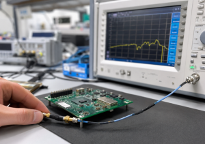
- Define prototype evidence: Plan measurements for rails, current, temperature, clocks, interfaces, transients, noise, EMC pre-compliance, and functional boundaries.
The approved design database and BOM should remain the source of truth; photographs or package resemblance are not reliable substitutes. For related guidance on maintaining values, manufacturer part numbers, packages, designators, alternates, and assembly data, see the PCB parts list workflow. Revisit the electronic components PCB selection process whenever requirements, layout, firmware, supplier, or production conditions change.
FAQs About Electronic Components PCB
Q1: Should every PCB component have a manufacturer part number?
A1: Production BOM lines should specify an exact orderable manufacturer part number. Generic values may be acceptable only when the controlled procurement specification defines all permissible ratings, packages, materials, and approved manufacturers.
Q2: Can I use the absolute maximum rating as the normal design value?
A2: No; design within the recommended operating conditions. Absolute maximum ratings are damage boundaries, not intended operating points, so include tolerance, transient, thermal, and reliability margin.
Q3: Is a pin-compatible IC automatically a safe substitute?
A3: No; require a form-fit-function comparison and risk-based validation. Pin compatibility does not prove matching logic thresholds, timing, analog performance, startup behavior, thermal limits, firmware registers, package geometry, or qualification.
Q4: Should I choose the smallest available component package?
A4: The smallest package is not always the lowest-risk production choice. Use it only when routing, thermal performance, placement, inspection, rework, and supplier capability support it.
Q5: What information should an approved component record contain?
A5: The record must provide unambiguous identity and revision control. Include the exact part number, manufacturer, description, value, ratings, tolerance, package, lifecycle, declarations, approved source, datasheet revision, alternates, and approval evidence.
Q6: How many alternative components should be approved?
A6: There is no universal number of approved alternatives. Qualify them where supply risk justifies the effort; a critical single-source item may need an architectural contingency, while common passives may support multiple prequalified sources.
Q7: Can prototype components be purchased from any available seller?
A7: Prefer authorized, traceable sourcing appropriate to the product risk. Development needs do not remove authenticity risk, so document any exception and avoid using uncertain parts for qualification or production decisions.
Q8: When should component selection be frozen?
A8: Freeze the production BOM only after all release evidence agrees. Requirements, schematic, footprint, worst-case analysis, DFM, sourcing, prototype results, and test plans must align; later changes require formal engineering change control.
Q9: Does RoHS status prove that a component meets all compliance needs?
A9: No; verify each applicable compliance obligation separately. RoHS addresses restricted substances within its scope, not electrical safety, automotive qualification, EMC performance, reliability, or end-product suitability.
Q10: What files should be sent to a PCBA supplier for component review?
A10: Send a complete, revision-aligned manufacturing data set. Include the released BOM, Gerber or ODB++, centroid file, assembly drawings, schematic when permitted, substitute rules, programming requirements, and test instructions.
Conclusion
Reliable PCB component selection connects circuit performance to manufacturability, verification, and supply continuity. Define requirements first, derive support networks from current manufacturer documents, verify ratings and footprints, plan for production and lifecycle risk, and control every substitute through documented change review. EBest Circuit can support the transition from design files and BOM review to PCB fabrication and PCBA preparation without replacing the customer’s component-design authority. If you are sourcing PCB/PCBA manufacturing, send your Gerber/ODB++, BOM, quantity, stackup, assembly, programming, and test requirements to sales@bestpcbs.com for engineering review and a quotation.
You may also like


Tags: Electronic Components PCB, PCB BOM, PCB Component Selection, PCB design components