





A high-power prototype board for a passive rectifier must carry capacitor-charging pulses without excessive voltage drop or overheating. It must also maintain the required insulation distances and provide guarded measurement access. Size the board from quantified input, load, surge, fault-energy, thermal, and test-duration limits.
In a capacitor-input rectifier, the diodes conduct near the AC waveform peaks rather than throughout each half-cycle. These narrow pulses raise RMS current, connector and copper loss, diode heating, inrush stress, and loop-induced overshoot above what an average DC-load calculation predicts.
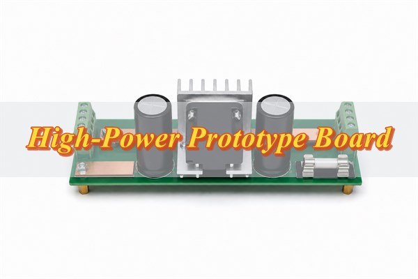
What Is a High-Power Prototype Board for a Passive Rectifier?
The board integrates the complete rectifier power path. It may carry a bridge or discrete diodes, a reservoir capacitor bank, fuses, inrush limiting, transient suppression, discharge resistors, current shunts, terminals, heat sinks, and guarded test points. Tests must establish output voltage and ripple, repetitive and surge-current capability, component temperatures, insulation integrity, and repeatable assembly.
What Input, Output, and Load Requirements Must Be Set Before Design?
Set worst-case electrical, thermal, and fault limits first. Nominal voltage and average output current do not cover input tolerance, waveform frequency, output ripple, startup charging, overload duration, cooling, enclosure conditions, or available short-circuit energy.
- AC input: Record minimum, nominal, and maximum RMS voltage; frequency; number of phases; source impedance; isolation method; and expected transient category.
- DC output: Define no-load and full-load voltage, allowable ripple, polarity, stored-energy limit, and whether the load tolerates an unregulated output.
- Load profile: Separate continuous current, repetitive peak current, short-duration overload, regenerative behavior, and load steps.
- Startup condition: State whether the capacitor bank may be discharged at turn-on and how often the unit can restart.
- Environment: Specify maximum ambient temperature, airflow, altitude, pollution degree, humidity, enclosure orientation, and nearby heat sources.
- Acceptance limits: Set maximum diode case temperature, capacitor surface temperature, busbar or terminal rise, output sag, ripple, and permitted test duration.
For a large transformer, mains-derived source, generator, or high-current secondary, define source isolation, available fault current, stored energy, discharge time, guarding, and the conditions that require protective earth.
For a sinusoidal single-phase source, bridge, and reservoir capacitor, the approximate no-load DC bus is the AC peak minus two conducting-diode drops: VDC ≈ √2 × VAC,RMS − 2VF. This estimate assumes the capacitor charges close to the waveform peak. Under load, transformer regulation, wiring resistance, diode conduction angle, capacitor ESR, and source impedance reduce the result. Use minimum input to check output compliance and maximum input to check voltage stress.
The load definition should also identify the actual current return. If a downstream converter draws narrow pulses, its local input capacitor and the rectifier capacitor interact through the wiring inductance. Testing only with a steady resistor may hide instability or peak-current stress that appears with the final electronic load.
How Do Passive Rectifier Topologies Affect High-Power Prototype Board Design?
Topology determines conduction loss, ripple, and loop geometry. Diode count and transformer use change the voltage and current stress on the source, semiconductors, copper, capacitors, and thermal system.
| Topology | Conducting Path | Transformer Requirement | Output Character | Board Impact |
| Half-wave | One diode per pulse | Single winding | Line-frequency ripple and poor source utilization | Simple layout, but larger filtering and asymmetric source current |
| Center-tapped full-wave | One diode and half the secondary per pulse | Center-tapped secondary with matched half-windings | Twice-line-frequency ripple | Lower diode-path drop, higher diode reverse-voltage demand, three winding connections |
| Single-phase bridge | Two diodes per pulse | Single secondary winding | Twice-line-frequency ripple | Compact general-purpose solution; two forward drops and concentrated bridge heating |
| Three-phase six-pulse bridge | Two diodes conduct at a time | Three-phase source | Six charging pulses per AC cycle and a shorter capacitor-discharge interval | Six diode branches, three phase terminals, phase-to-phase spacing, and package-dependent heat concentration |
A single-phase bridge is often practical because it needs no center tap and uses both half cycles. Two diode drops can nevertheless create substantial loss at high current. For a continuous DC load, Pbridge ≈ 2 × VF × Iload is only a first estimate. Final loss should use the device’s forward-voltage curve and the measured or simulated diode-current waveform because capacitor-input conduction is pulsed.
A three-phase bridge spreads conduction among six devices and raises ripple frequency, but also requires six high-current branches. Its phase terminals, fusing, heat-sink isolation, current sensing, and guarded probe points must accommodate phase-to-phase voltage and the physical spacing of three input conductors.
Which Construction Method Is Suitable for a High-Power Prototype Board?
Match construction to current, heat, voltage, and mechanics. A two-layer FR-4 high-power prototype board is suitable only when its finished copper geometry, joints, spacing, and measured temperature rise meet the design limits. As current or stored energy increases, heavy copper, bolted busbars, or a hybrid board-and-chassis structure may provide a more controllable current path.
Solderless breadboards, generic stripboard, and loose jumper wires should be excluded unless their documented current capacity, contact resistance, insulation spacing, and fault behavior cover the intended test. For higher-energy work, use a purpose-built PCB, a bolted fixture, or a chassis-mounted assembly with defined conductors and guarded terminals.
| Construction | Current Path | Modification Boundary | Thermal Path | Appropriate Validation Scope | Main Limitation |
| Standard FR-4 PCB | Wide traces and planes | Components can be reworked; copper geometry requires a new board | Trace and terminal temperature depend on finished copper geometry, board construction, and airflow | Topology and layout when measured conductor and terminal temperatures meet the limits | Trace neck-downs, vias, and connectors may set the current limit |
| Heavy copper PCB | Thicker etched copper | Components can be reworked; copper geometry and spacing require new fabrication | Thicker copper lowers trace resistance at the same width; spreading remains layout-dependent | Compact high-current paths after fabricator DFM and thermal validation | Etching, spacing, soldering, and cost need early DFM review |
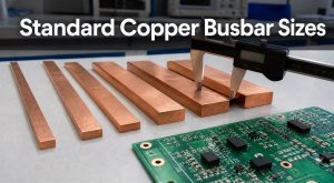
| PCB with bolted busbars | Busbars carry the main current; PCB supports control and connection | Bolted bars are replaceable when joints remain accessible | Resistance and heating depend on bar material, cross-section, overlap, surface condition, and joint torque | When etched-copper loss or board area is limiting and bolted joints can be qualified | Joint resistance, torque, flatness, and mechanical support require control |
| Chassis-mounted power stage | Wires or busbars between mounted components | Wiring and busbars can be reworked; mounting changes require mechanical review | Power packages can couple directly to a heat sink or chassis through a specified interface | Large packages, substantial dissipation, or guarded high-energy testing | Less compact and harder to convert directly into production PCB geometry |
| Solderless or generic stripboard | Spring contacts or narrow strips | Connections are easy to change but are not a repeatable power interconnect | Contact resistance and temperature rise are uncontrolled unless the manufacturer rates the exact assembly | Only low-energy checks within documented ratings | Usually lacks verified spacing, current capacity, and fault-interruption behavior for this application |
Match the production current path to the measurement objective. A thin-trace PCB cannot validate the voltage drop or temperature rise of a production busbar, while an oversized hand-built busbar can hide final routing, joint, and assembly constraints.
How Should Rectifier Diodes, Capacitors, and Protection Components Be Selected?
Select parts from actual waveforms and temperatures. Use manufacturer curves at the intended case and ambient temperatures. Forward drop, allowable current, surge withstand, thermal resistance, capacitor ripple rating, expected life, and fault survival all change with waveform and cooling conditions.
- Reverse voltage: Rate each diode above the highest repetitive reverse voltage, including source tolerance and credible transients.
- Forward current: Check average, RMS, and repetitive peak current at the intended case temperature rather than using the headline current alone.
- Surge current: Compare the non-repetitive surge rating with capacitor charging and fault conditions, including the waveform duration stated in the datasheet.
- Forward loss: Use the forward-voltage curve at the expected pulse current to estimate diode heating.
- Capacitor ripple: Confirm RMS ripple-current capability, ESR, temperature rating, lifetime model, voltage margin, and mechanical vent clearance.
- Protection coordination: Select fuses, breakers, NTC limiters, precharge resistors, MOVs, TVS devices, and discharge resistors as one energy-control strategy.
For a single-phase, full-wave, line-frequency capacitor-input supply, a first estimate is C ≈ Iload ÷ (2 × fline × ΔV), where ΔV is the permitted capacitor discharge between charging peaks. The approximation assumes nearly constant load current and does not predict conduction angle, charging-current peaks, ESR heating, transformer copper loss, or startup surge. Confirm peak and RMS currents by waveform simulation or staged measurement.
Capacitor ESR loss is estimated by Pripple ≈ Iripple,RMS2 × ESR. ESR changes with frequency, temperature, and aging, so use the selected series’ data at the relevant conditions. Parallel capacitors can share ripple and reduce effective ESR only when copper geometry, part tolerance, thermal exposure, and connection resistance support balanced current.
An NTC limiter is simple, yet it may remain hot and provide little protection during a rapid restart. A resistor-plus-bypass relay or contactor can provide controlled precharge for a larger capacitor bank, but the bypass timing and failure state must be tested. The fuse must interrupt the available fault current at the applied voltage; its current rating alone does not prove safe interruption.
How Should Copper Weight, Trace Width, Vias, and Busbars Carry High Current?
Size the entire current path, not only its copper traces. Include planes, plated holes, solder joints, terminals, and busbars in resistance, temperature-rise, voltage-drop, fault-current, and manufacturability checks. IPC-2152 data can support high-current PCB conductor estimates, but IPC lists the document as no longer maintained. It cannot replace the applicable product standard, fabricator data, or prototype thermal testing.
Calculate the DC resistance of each uniform copper segment from R = ρL ÷ (w × t), using copper resistivity at the relevant temperature. Estimate conductor loss with P = IRMS2R. Include charging pulses in the RMS value and add via, solder-joint, fuse-clip, connector, cable-lug, and busbar-interface resistance instead of treating etched copper as the whole path.
- Copper weight: Select finished copper thickness with the fabricator; plated outer layers and etched feature tolerances affect the final geometry.
- Trace width: Use planes or broad polygons for power paths, but preserve required spacing and avoid neck-downs at pads and terminals.
- Layer sharing: Parallel copper on multiple layers can lower resistance only when current transfers through a deliberate, adequately plated via pattern.
- Via arrays: Treat each via as a plated barrel with manufacturing tolerance; distribute arrays to avoid a single hot transfer point.
- Busbar joints: Control overlap area, surface condition, flatness, washer stack, torque, insulation, and strain relief.
- Current measurement: Use a defined shunt or four-wire measurement points instead of estimating path resistance from distant voltage nodes.
Do not use solder buildup to compensate for undersized copper; solder has higher resistivity than copper and an uncontrolled finished thickness. Specify any external copper bar or wire reinforcement in the fabrication and assembly drawings with its material, cross-section, attachment, insulation, and inspection criteria.
How Should the High-Current Rectifier Loop and Power Components Be Laid Out?
Minimize the bridge-to-capacitor charging-loop area. In a capacitor-input rectifier, this pulsed loop runs from the transformer or AC connector through the conducting diode pair to the reservoir capacitor and back to the source. Excess inductance increases ringing and overshoot; unequal branch impedance distorts current sharing.
- Trace the pulse loop. Mark the source terminal, conducting diode pair, reservoir-capacitor terminals, and source return on the schematic and PCB. This identifies the copper that must enclose the smallest practical area.
- Couple bridge and capacitor. Place the bridge DC terminals and reservoir-capacitor terminals in the same power region with direct, wide copper between them. Do not send this path through a connector, test point, long neck-down, or board-edge detour.
- Take the load at the capacitor. Route both outgoing DC conductors from the capacitor connection points. A load takeoff in the middle of the charging path makes pulse current share copper with load current and adds ripple-related voltage error.
- Pair forward and return paths. Use adjacent planes or closely spaced conductors with uninterrupted reference geometry where insulation rules allow. Avoid slots, split copper, and widely separated routes that enlarge loop area.
- Control every layer transfer. Use distributed via arrays and full-width pad entries at high-current transitions. A single via, thermal-relief spoke, or pad neck-down can dominate resistance even when the surrounding plane is wide.
- Balance parallel branches. Match copper length, width, via count, joint count, and cooling for parallel diodes or capacitors. Place shared connection points symmetrically; equal part numbers do not correct unequal interconnect impedance.
- Place protection in series with the fault path. Locate the fuse, inrush limiter, or precharge path before the vulnerable downstream copper. Keep hot limiters and fuse clips away from electrolytic capacitors, plastic connectors, and temperature-sensitive sensing parts.
- Separate sensing from power joints. Run Kelvin traces from the actual diode, shunt, or capacitor terminals. Do not sense through a bolted joint, fuse clip, connector pin, or shared high-current pad whose resistance changes with temperature and torque.
- Check the assembled three-dimensional path. Verify that heat-sink tabs, mounting screws, washers, standoffs, and busbars cannot short a node, reduce creepage, obstruct airflow, or place mechanical load on a solder joint.
Measure ringing before selecting a snubber. Probe at the bridge or diode terminals with a suitably rated differential probe and the shortest practical connection. Record peak voltage and ringing frequency, then calculate and tune the RC network for that measured parasitic response. Recheck diode stress, snubber-component temperature, and input current because a generic capacitor across the bridge can increase loss without controlling the actual resonance.
How Should Creepage, Clearance, and Heat Dissipation Be Controlled?
Set insulation spacing and thermal paths from verified limits. Clearance is the shortest distance through air; creepage is the shortest distance along an insulating surface. Working voltage, impulse stress, insulation type, pollution degree, material group, coating, and altitude determine the required values.
Start with the product’s governing safety standard and high-voltage PCB insulation architecture. For equipment within its scope, IEC 60664-1:2020 with Amendment 1:2025 provides insulation-coordination principles for low-voltage systems; the applicable end-product standard still controls the final design. Identify hazardous, accessible, earthed, floating, and isolated nets, then inspect conductor edges, component leads, heat-sink hardware, fuse clips, mounting holes, slots, connector bodies, and the assembled three-dimensional path. A routing rule alone cannot find every reduced distance.
For a steady-state first estimate, use TJ ≈ TA + Ploss × RθJA only when the datasheet’s board, copper, and airflow conditions resemble the assembly. A heat-sunk device is better modeled with junction-to-case, interface, and sink-to-ambient resistances. Copper spreading, thermal vias, a heat sink, a chassis interface, or forced air must be represented in the prototype and confirmed by measurement.
- Heat separation: Keep hot bridge heat sinks and precharge resistors away from electrolytic capacitors and plastic connectors.
- Thermal vias: Use an array only when the receiving layer has enough copper area to spread the heat.
- Heat-sink isolation: Confirm whether the package tab is electrically live and specify any pad, shoulder washer, or isolated mounting hardware.
- Ventilation: Preserve the capacitor vent path and the airflow channel through heat-sink fins.
- Temperature sensing: Attach thermocouples consistently and account for measurement error from airflow, adhesive, and electrical potential.
How Should a High-Power Prototype Board Be Fabricated and Assembled?
Preserve copper, spacing, joint quality, and support. Reject over-etched neck-downs, inadequate hole plating, incomplete wetting on heavy copper, loose terminals, board warpage, and unsupported capacitors.
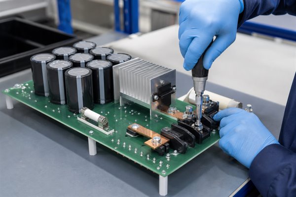
- Release controlled production data. Supply Gerber or ODB++, drill data, stackup, finished copper requirements, netlist, fabrication notes, and a drawing that identifies controlled high-current features.
- Complete power-board DFM. Review heavy-copper etching, minimum spacing after etch compensation, plated-hole aspect ratio, annular rings, solder-mask dams, slots, and finished board thickness.
- Verify exact footprints. Check the selected diode, bridge, capacitor, fuse, terminal, shunt, heat sink, and mounting hardware against their current datasheets.
- Define measurable acceptance evidence. Use coupons or inspection records for finished copper, neck-down width, hole plating, and critical insulation dimensions when the risk requires verification.
- Inspect the bare board. Check opens, shorts, copper defects, hole quality, cleanliness, solder-mask registration, and dimensions before components conceal the features.
- Control assembly sequence. Install low-profile parts before power semiconductors, terminals, capacitors, busbars, heat sinks, and mechanically retained components.
- Qualify the soldering process. Deliver enough heat to wet heavy copper without scorching laminate, degrading parts, or leaving incomplete through-hole joints.
- Control bolted joints. Apply the specified torque and approved washer, thread-locking, and insulation stack to electrical terminals and heat-sink hardware.
- Inspect the finished assembly. Verify polarity, diode orientation, capacitor vent clearance, solder wetting, busbar alignment, cleanliness, and conductor spacing.
- Start with low-energy checks. Complete continuity, isolation, resistance, and low-voltage functional tests before connecting the intended high-energy source.
Record every manual reinforcement, selective-soldering requirement, torque value, thermal compound, insulating pad, staking material, and inspection point. Undocumented technician adjustments make the assembly result non-repeatable.
How Does a Passive Rectifier Prototype Perform Under Full Load?
A passing prototype must meet every preset limit. Reaching the target current for a few seconds does not prove continuous capability. Test cold start, thermal soak, minimum and maximum input, intended load dynamics, restart behavior, and safe shutdown against predetermined electrical, thermal, and protection limits.
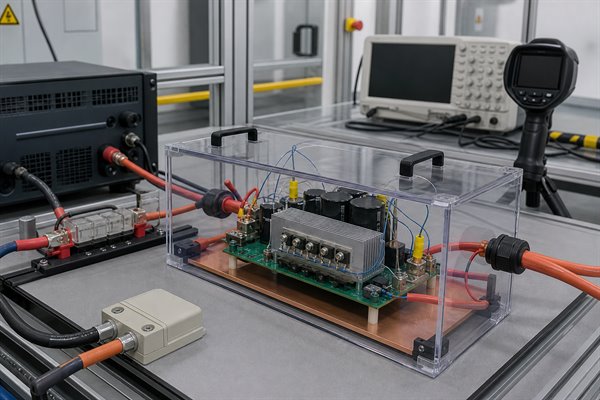
- Secure the test area. Inspect the de-energized setup, discharge capacitors, verify polarity, confirm protective earth where applicable, and place the board behind a suitable guard.
- Limit first-energization energy. Use a current-limited isolated source or controlled low-energy source with the intended fuse and precharge path installed.
- Establish the no-load baseline. Measure DC voltage, polarity, residual current, discharge time, and unexpected heating before adding load.
- Increase load in planned steps. Record RMS input current, DC output voltage, ripple, diode or bridge temperature, capacitor temperature, and terminal temperature at each step.
- Check current-path balance. Measure voltage drop across high-current joints and compare parallel branch currents when the design uses parallel devices or capacitors.
- Complete the thermal soak. Hold full load until temperatures approach a stable plateau or the planned time limit is reached; stop at any predefined safety limit.
- Test the operating corners. Repeat at minimum and maximum specified input with the real load profile or a representative dynamic electronic-load program.
- Verify restart behavior. Test cold restart, hot restart, and the permitted restart interval to confirm inrush-limiter recovery and fuse coordination.
- Capture transients safely. Measure switching or commutation overshoot with correctly rated probes and a controlled grounding method.
- Inspect after shutdown. Verify capacitor discharge, then check discoloration, odor, loose hardware, solder damage, insulation tracking, and changed joint resistance.
Efficiency alone can hide a localized defect. A board may show acceptable total loss while one fuse clip, via transition, or busbar joint runs much hotter than adjacent copper. Thermal images are useful for locating patterns, but emissivity and reflections can distort readings; confirm critical points with an appropriate contact measurement.
Why Do High-Power Prototype Boards Fail, and How Can the Design Be Improved?
Correct the measured mechanism, not only the damaged part. Common causes include underestimated pulse current, concentrated resistance, insufficient insulation, poor heat transfer, and applying full energy before low-power checks.
| Failure Symptom | Likely Mechanism | Verification | Design Improvement |
| Bridge overheats although DC load current is below the catalog headline rating | High forward drop, narrow charging pulses, inadequate heat sink, or poor interface | Measure diode waveform, case temperature, and heat-sink temperature | Recalculate pulsed loss, improve thermal interface, or select a lower-loss topology or package |
| Fuse opens during startup | Capacitor inrush exceeds fuse time-current behavior | Capture startup current and compare with fuse curve | Add coordinated precharge or choose a correctly rated fuse without weakening fault protection |
| Capacitors run hot | Excess ripple current, high ESR, unequal sharing, or bridge heat exposure | Measure branch ripple and capacitor surface temperature | Use suitable ripple-rated parts, symmetric copper, more separation, or a revised filter |
| Copper or terminal discolors | Neck-down, poor solder joint, loose bolted joint, or undersized connector | Four-wire voltage-drop and thermal comparison | Increase cross-section, correct joint design, specify torque, and add mechanical support |
| Overshoot or ringing damages diodes | Commutation-loop inductance, diode reverse recovery, or uncontrolled parasitic resonance | Use a safe high-bandwidth differential measurement | Shrink the loop and tune a measured snubber rather than adding a generic capacitor |
| Arcing or carbon tracking | Inadequate creepage or clearance, contamination, altitude, or transient stress | Inspect the assembled three-dimensional path and governing standard inputs | Increase spacing, add a justified slot or barrier, improve cleanliness, and reassess insulation coordination |
After any change, repeat the tests affected by that change. Widening a busbar may alter current sharing; moving a capacitor may enlarge the charging loop; adding a heat sink may reduce creepage; changing the NTC may alter hot-restart protection. Preserve waveform captures, temperatures, input conditions, load steps, photos, and revision identifiers so the next prototype is based on evidence rather than memory.
FAQs About High-Power Prototype Boards for Passive Rectifier Design and Testing
Q1: Can a solderless breadboard be used for an initial high-power rectifier test?
A1: No—use it only for isolated, low-energy checks within its documented ratings. Spring contacts and narrow internal strips generally lack documented high-current and insulation performance for this application. Use a purpose-built PCB, bolted fixture, or chassis-mounted test assembly with fusing and guarded terminals.
Q2: Should the high-power prototype board use the same copper construction as the production board?
A2: Match the production current path as closely as the test objective requires. A thin-copper prototype cannot validate the temperature rise of a future heavy-copper board, while an oversized busbar can conceal production constraints. Document every construction difference and limit the conclusions drawn from it.
Q3: Is a bridge rectifier’s catalog current rating enough for selection?
A3: No—the usable current depends on waveform and case temperature. Check average, RMS, repetitive peak, and non-repetitive surge current, plus forward-voltage and thermal curves. Capacitor-input supplies can produce diode-current peaks well above the DC load current.
Q4: When is a busbar preferable to thicker PCB copper?
A4: A busbar is favored when etched copper cannot meet loss, temperature, space, or joint requirements economically. It can provide a low-resistance path, but overlap area, torque, flatness, insulation, strain relief, and inspection must be designed rather than improvised.
Q5: How can current sharing between parallel rectifier diodes be checked?
A5: Measure each branch under thermal equilibrium with matched low-inductance sensing. Compare branch voltage drop or calibrated shunt current while controlling copper symmetry and cooling. Static forward-voltage matching alone does not prove sharing because temperature changes the diode characteristic.
Q6: Does conformal coating automatically allow smaller creepage distance?
A6: No—spacing reduction requires support from the governing standard and a qualified coating process. Coating type, coverage, cleanliness, cure, inspection, pollution degree, and long-term environment matter. Do not treat generic coating as a substitute for insulation coordination.
Q7: What data should be logged during a thermal soak?
A7: Record input, load, airflow, ambient, component temperatures, and elapsed time together. Include bridge case, heat sink, capacitor body, fuse, terminal, and the hottest copper joint. A temperature without its electrical and cooling conditions cannot support a design limit.
Q8: How should stored energy be handled after a test?
A8: Use a designed discharge path and verify voltage before touching the board. The discharge resistor must be rated for initial power and total energy, and the waiting time must be defined. A visual power indicator is helpful but does not replace a voltage measurement.
Q9: What files should be sent for a rectifier prototype quotation?
A9: Send Gerber or ODB++, drill data, BOM, assembly drawings, stackup, copper requirements, and test criteria. Also include peak and continuous current, maximum voltage, thermal limits, busbar drawings, torque requirements, insulation notes, and any programmed load-test sequence.
Q10: Can full-load testing be replaced by simulation?
A10: No—simulation narrows risk, but hardware testing validates parasitics, joints, cooling, and assembly variation. Use simulation to estimate conduction pulses, ripple, loss, and transients, then confirm them through staged, current-limited testing before applying the maximum-energy condition.
Conclusion
Release the design only after staged energization and a full-load thermal soak. Confirm output voltage, ripple, component temperatures, joint voltage drop, current sharing, overshoot, insulation integrity, restart behavior, and protection operation at the specified input and load limits.
For a high-power prototype board quotation from EBest Circuit, send your Gerber/ODB++, BOM, quantity, stackup, copper and busbar requirements, assembly drawings, and test requirements to sales@bestpcbs.com.
You may also like

Tags: high-power prototype board, high-power prototype testing, high-power rectifier layout, high-power rectifier prototype