An SOIC package is one of the most common surface-mount IC packages used in PCB and PCBA projects. It is larger than many modern fine-pitch IC packages, but it is still widely used because it is easy to source, easy to inspect, relatively simple to assemble, and suitable for many industrial, consumer, power, communication, and control boards.
In this article, SOIC means Small Outline Integrated Circuit. It does not refer to TSMC SoIC advanced semiconductor packaging. For PCB assembly projects, the practical questions are usually about SOIC body size, pin pitch, footprint, soldering, pin 1 direction, BOM consistency, and SMT inspection.
EBest Circuit (Best Technology) supports PCB fabrication, BOM sourcing, SMT assembly, inspection, testing coordination, and small-batch PCBA production. If your project includes SOIC ICs, SOIC-8 packages, SOP/SSOP/TSSOP alternatives, or footprint questions, you can send your Gerber files, BOM, CPL, assembly drawing, and datasheets to sales@bestpcbs.com for engineering review before production.
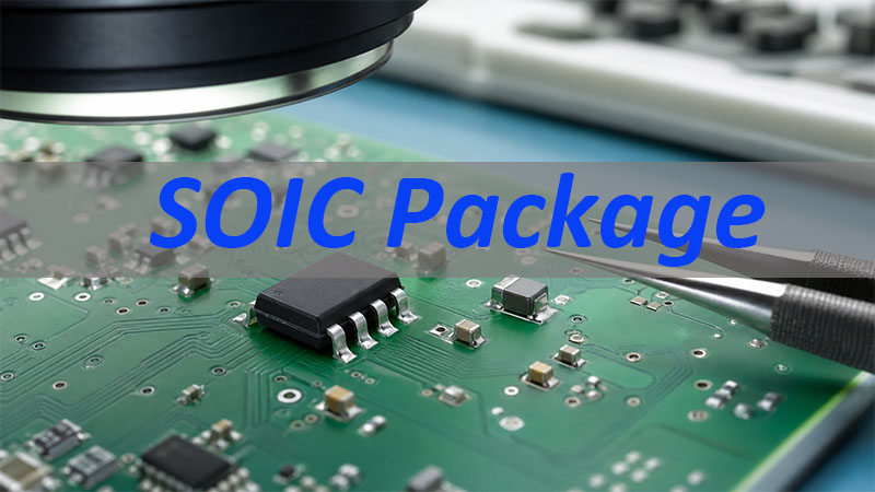
What Is an SOIC Package?
An SOIC package is a surface-mount integrated circuit package with leads on two opposite sides of the IC body. The leads usually have a gull-wing shape, which means they bend outward and down toward the PCB pads.
SOIC packages are commonly used for:
- operational amplifiers
- EEPROM and flash memory
- interface ICs
- drivers
- sensors
- power management ICs
- logic ICs
- microcontrollers
- communication ICs
Compared with through-hole DIP packages, SOIC packages save PCB space and support automated SMT assembly. Compared with smaller packages such as QFN, WSON, or BGA, SOIC packages are easier to visually inspect and rework because the leads are exposed.
For PCBA projects, “SOIC package” should not be treated as a complete ordering description. The BOM and datasheet should also define pin count, pitch, body width, package variant, manufacturer part number, and footprint.
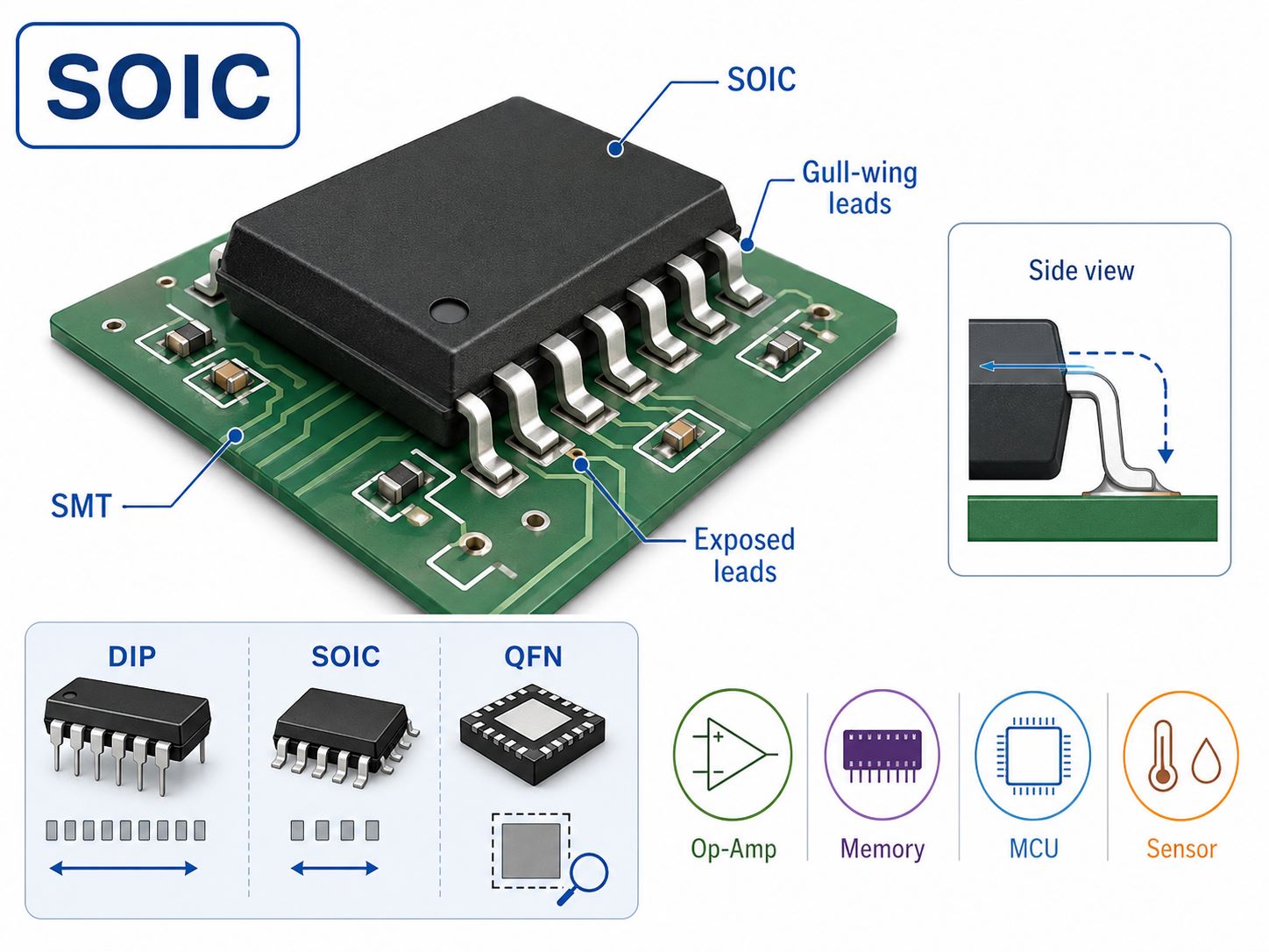
SOIC Full Name: Small Outline Integrated Circuit
The full name of SOIC is Small Outline Integrated Circuit.
The name describes its role clearly:
| Term | Meaning |
|---|---|
| Small Outline | Smaller than traditional through-hole DIP packages |
| Integrated Circuit | Used for IC components |
| Package | Physical component body and lead structure |
SOIC is part of the larger small-outline package family. Related package names may include SOP, SSOP, TSSOP, MSOP, and SOIC-W.
In practice, engineers and suppliers may use slightly different naming styles. You may see:
- SOIC
- SO
- SOIC-8
- SO-8
- SOIC-N
- SOIC-W
- SOP
- narrow SOIC
- wide SOIC
This is why the exact datasheet matters. A BOM line that says only “SOIC” may not be enough for PCB footprint and electronic PCBA.
SOIC IC Package Structure and Lead Style
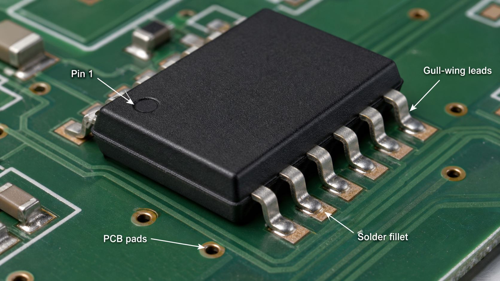
An SOIC IC package usually has a molded rectangular body and metal gull-wing leads on two sides.
Important physical features include:
- package body length
- package body width
- package height
- lead pitch
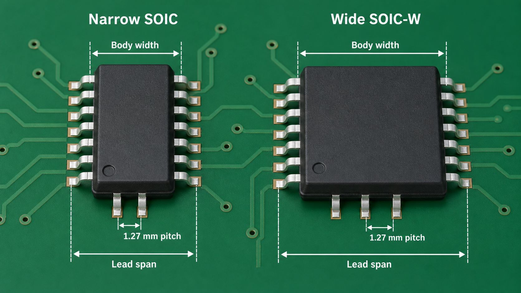
- lead span
- lead width
- pin count
- pin 1 mark
- seating plane
- coplanarity
The exposed gull-wing leads make SOIC easier to inspect than many leadless packages. During PCBA inspection, the solder joints can often be checked by AOI or visual inspection.
However, SOIC packages still have assembly risks. If the footprint is wrong, if the stencil aperture is not suitable, or if the component orientation is incorrect, defects may appear during SMT.
Common risks include:
- solder bridging between leads
- insufficient solder fillet
- skewed placement
- lifted leads
- wrong pin 1 orientation
- footprint mismatch
- poor wetting
- rework damage
For this reason, SOIC should be checked in the BOM, footprint, CPL file, assembly drawing, and datasheet before SMT starts.
SOIC-8 Package and Common Pin Counts
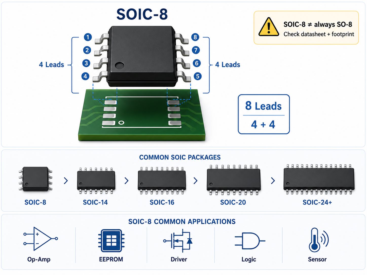
The SOIC-8 package is one of the most common SOIC formats. It has 8 leads, with 4 leads on each side.
SOIC-8 is often used for:
- op-amps
- EEPROMs
- small power ICs
- interface chips
- MOSFET drivers
- logic ICs
- isolated drivers
- sensor ICs
Other SOIC pin counts may include:
| Package | Common Use |
|---|---|
| SOIC-8 | Small analog, memory, logic, interface ICs |
| SOIC-14 | Logic, drivers, control ICs |
| SOIC-16 | Interface, logic, mixed-signal ICs |
| SOIC-20 | Larger ICs and driver packages |
| SOIC-24+ | Higher pin-count small-outline ICs |
One important warning: SOIC-8 and SO-8 are not always identical in every datasheet. Some manufacturers may use similar naming for different body widths or land patterns. Before PCB layout or PCBA assembly, the package drawing in the component datasheet should be checked against the PCB footprint.
SOIC Package Dimensions and Body Widths
SOIC package dimensions vary by manufacturer, pin count, and package family. The same “SOIC” name may not always mean the same body width.
Common SOIC-related width styles include:
| Type | Typical Meaning |
|---|---|
| Narrow SOIC | Common smaller-width SOIC body |
| Wide SOIC / SOIC-W | Wider body, often used for isolation or larger pin counts |
| SOIC-N | Narrow version in some datasheets |
| SOIC-W | Wide version in some datasheets |
| SOP | Similar small-outline family, naming depends on standard and supplier |
For PCB and PCBA, the most important point is not memorizing one dimension. The real point is to match:
- exact manufacturer part number
- package drawing
- body width
- lead pitch
- lead span
- land pattern
- courtyard clearance
- pin 1 orientation
A common SOIC lead pitch is 1.27mm, but engineers should not assume every SOIC-like package uses the same pitch. SSOP, TSSOP, MSOP, and other small-outline packages may use smaller pitch values.
SOIC vs SOP Package: Are They the Same?
SOIC and SOP are closely related, but they are not always used in exactly the same way.
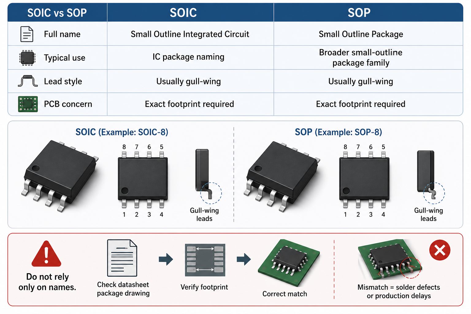
In many practical sourcing and assembly discussions, SOIC and SOP may refer to similar small-outline IC packages with gull-wing leads. However, package naming can depend on the manufacturer, region, and standard.
| Item | SOIC | SOP |
|---|---|---|
| Full name | Small Outline Integrated Circuit | Small Outline Package |
| Typical use | IC package naming | Broader small-outline package family |
| Lead style | Usually gull-wing | Usually gull-wing |
| PCB concern | Exact footprint required | Exact footprint required |
For PCBA production, the safe approach is simple: do not rely only on the words SOIC or SOP. Use the datasheet package drawing and approved footprint.
If a BOM lists an IC as SOP but the PCB footprint is SOIC, or the supplier substitutes one package for another, the part may not fit the pads correctly. This can cause soldering defects or production delays.
SOIC vs SSOP and TSSOP Package
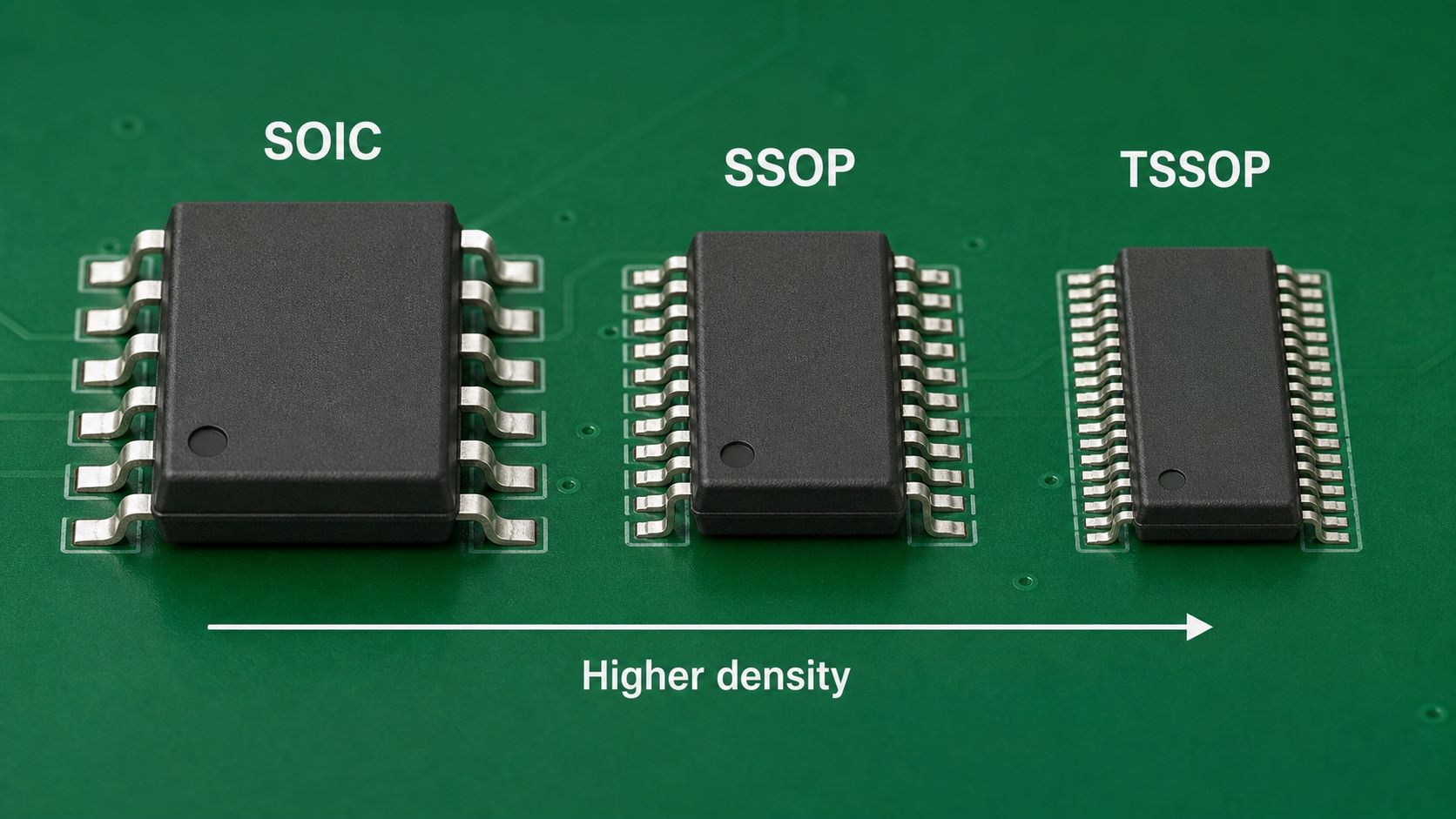
SOIC, SSOP, and TSSOP are all surface-mount IC package families, but they differ in size, pitch, and assembly difficulty.
| Package | General Feature |
|---|---|
| SOIC | Larger pitch, easier inspection and rework |
| SSOP | Smaller than SOIC, higher density |
| TSSOP | Thinner and smaller pitch, more compact layout |
| MSOP | Smaller package for compact circuits |
Compared with SOIC, SSOP and TSSOP can save board space, but they usually require tighter SMT process control. Smaller pitch increases the risk of solder bridging, placement deviation, and inspection difficulty.
For engineering and purchasing teams, package changes should not be treated as simple substitutions. Replacing an SOIC with SSOP or TSSOP may require:
- new PCB footprint
- new stencil aperture design
- updated CPL data
- revised assembly drawing
- solder paste process review
- AOI program update
- possible rework method changes
EBest Circuit can help review whether the BOM, PCB footprint, and SMT data match the selected package before production.
SOIC PCB Footprint and Land Pattern Checks
The SOIC PCB footprint is one of the most important checks before PCBA assembly.
A good footprint should match the component datasheet and assembly requirement. It should consider:
- pin pitch
- pad length
- pad width
- toe fillet
- heel fillet
- side fillet
- solder mask opening
- silkscreen clearance
- courtyard area
- pin 1 mark
- nearby component clearance
- rework access
Common footprint problems include:
- using a narrow SOIC footprint for a wide SOIC part
- incorrect lead pitch
- wrong pin 1 orientation
- pads too short for reliable solder fillet
- silkscreen overlapping pads
- insufficient clearance for inspection or rework
- CPL rotation not matching assembly drawing
For prototype builds, these issues may only affect a few boards. For batch production, the same issue can repeat across the entire lot. That is why footprint review before SMT is much cheaper than rework after assembly.
SOIC SMT Assembly Process and Soldering Risks
SOIC packages are usually assembled through standard SMT processing.
A practical SMT flow may include:
- PCB baking when required
- solder paste printing
- SPI inspection
- pick-and-place
- reflow soldering
- post-reflow inspection
- AOI
- manual inspection
- rework if needed
- functional test coordination
- packing
SOIC packages are generally easier to assemble than very fine-pitch ICs, but soldering problems can still occur.
Common SOIC assembly risks include:
- solder bridge between adjacent leads
- insufficient solder volume
- component skew
- lifted leads
- poor wetting
- wrong orientation
- flux residue around leads
- heat damage during rework
Inspection should focus on:
- pin 1 direction
- lead alignment
- visible solder fillets
- bridging
- missing solder
- lead coplanarity
- correct part number
- polarity or orientation marks
If the SOIC package is close to tall capacitors, connectors, shields, or mechanical parts, rework access should also be considered.
How EBest Circuit Reviews SOIC Package Before PCBA
SOIC package issues are usually preventable when the files are reviewed before production.
Before PCBA assembly, EBest Circuit can help check:
- BOM package description
- manufacturer part number
- datasheet package drawing
- PCB footprint
- pin 1 marking
- CPL rotation
- assembly drawing
- stencil and solder paste requirements
- SMT placement direction
- inspection notes
- approved alternates
This is especially useful when a project includes similar packages such as SOIC, SOP, SSOP, TSSOP, MSOP, or SOIC-W. These packages may look similar in the BOM, but they are not automatically interchangeable on the PCB.
EBest Circuit supports PCB fabrication, component sourcing, SMT assembly, through-hole assembly, inspection, testing coordination, and small-batch production. For customers preparing SOIC-based PCB assemblies, the goal is to catch package, footprint, and orientation risks before boards enter SMT.
FAQs About SOIC Package
1. What is an SOIC package?
An SOIC package is a surface-mount IC package with gull-wing leads on two sides. It is commonly used for integrated circuits in PCB assembly.
2. What does SOIC stand for?
SOIC stands for Small Outline Integrated Circuit.
3. Is SOIC the same as SOP?
They are closely related, but not always identical. The exact package drawing and footprint should be checked before PCB layout or SMT assembly.
4. What is SOIC-8?
SOIC-8 is an 8-pin SOIC package, commonly used for op-amps, EEPROMs, drivers, logic ICs, and small interface chips.
5. What is the difference between SOIC and TSSOP?
TSSOP is usually thinner and has a smaller lead pitch than SOIC. It saves board space but requires tighter SMT process control.
6. What should be checked before assembling SOIC components?
Check the BOM, manufacturer part number, datasheet package drawing, PCB footprint, pin 1 direction, CPL rotation, stencil data, and assembly drawing.
7. Can SOIC parts be hand soldered?
Many SOIC packages can be hand soldered or reworked with proper tools, but production assembly usually uses SMT reflow.
8. Is TSMC SoIC the same as SOIC package?
No. TSMC SoIC refers to advanced semiconductor packaging technology. This article discusses SOIC as Small Outline Integrated Circuit package for quick PCB fabrication and turnkey PCBA assembly service.
To conclude, the SOIC package remains widely used because it offers a practical balance between board space, assembly reliability, inspection access, and component availability. It is easier to inspect than many leadless packages and smaller than traditional through-hole DIP packages.
For bare printed circuit board and electronic PCBA assembly projects, the package name alone is not enough. Engineers and buyers should confirm the exact SOIC variant, pin count, body width, lead pitch, footprint, pin 1 direction, and assembly notes before production.
If your project includes SOIC ICs, SOIC-8 parts, SOP/SSOP/TSSOP alternatives, or package-to-footprint questions, please send your Gerber files, BOM, CPL, assembly drawing, and component datasheets to sales@bestpcbs.com. EBest Circuit can help review the manufacturing and assembly details before SMT, so package-related problems are caught earlier.