
Multilayer PCB manufacturing builds several copper and dielectric layers into one controlled circuit board, so the main risk is not only making more layers. The real risk is whether the stackup, material, registration, lamination, drilling, plating, inspection and assembly plan are controlled before production starts.
For buyers, a multilayer PCB quote should answer more than price and delivery. It should show whether the board can be fabricated, assembled, tested and repeated without late stackup changes, missing impedance details, unstable material choices or unclear inspection scope. EBest Circuit reviews multilayer PCB fabrication, PCBA, BOM, CPL and test expectations together when a project needs a practical quote path.
Is your multilayer PCB project stuck before a reliable quote?
Multilayer PCB projects often slow down when the files look complete, but the manufacturing assumptions are still open.
- The stackup does not define layer order, dielectric targets, copper weight or impedance requirements clearly enough for fabrication.
- The board needs 8 or more layers, but material Tg, lamination risk and thickness tolerance have not been checked early.
- Drill size, aspect ratio, annular ring and plating expectations are reviewed after the quote, forcing another design revision.
- Assembly files arrive separately from fabrication files, so test points, panelization, fiducials and component clearance are not checked together.
- The first quote looks fast, but later stackup confirmation, material substitution or DFM changes delay the actual build.
EBest Circuit helps buyers turn multilayer PCB files into a controlled manufacturing plan:
- We review Gerber or ODB++ files, drill files, stackup notes, copper, material, surface finish and board thickness before quote assumptions are locked.
- For FR-4 and high-Tg multilayer projects, we check whether the layer count and material route match the board’s thermal, reliability and production needs.
- We connect fabrication review with PCBA, BOM, CPL, test points and packaging when the customer needs assembled boards rather than bare PCBs only.
- We flag DFM issues early, including tight spacing, drill risk, solder mask bridge limits, panelization, fiducials and inspection requirements.
- We build the quote around real project files, quantities and target delivery plans, so buyers can compare suppliers with fewer hidden assumptions.
What Multilayer PCB Manufacturing Must Control
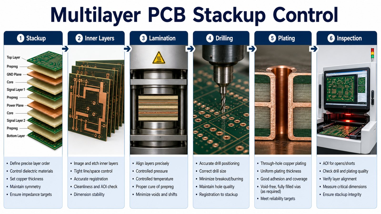
Multilayer PCB manufacturing must control the stackup, inner layers, dielectric materials, lamination, drilling, plating, surface finish and inspection as one connected process.
A 4-layer, 6-layer, 8-layer or higher-layer board can fail commercially even when each separate process step looks normal. The stackup affects impedance, copper balance, board thickness, drilling and assembly. The lamination cycle affects registration and dielectric stability. Drill and plating choices affect reliability through the plated holes. That is why a multilayer PCB quote should start with the stackup and manufacturing route, not only the finished board size.
When Multilayer PCB Projects Get Delayed Before Production
Most multilayer PCB delays happen before the factory build, when stackup, material, drill, copper or assembly requirements are still unclear.
| Delay Point | What Usually Causes It | How to Reduce the Risk |
|---|---|---|
| Stackup approval | Layer order, dielectric thickness or impedance target is missing | Send stackup notes or ask for a manufacturable stackup review |
| Material choice | Standard FR-4 is assumed where high-Tg or special material may be needed | Share operating temperature, reliability needs and application context |
| Drilling and plating | Small holes, high aspect ratio or tight annular rings are checked late | Review drill table, finished hole size and board thickness together |
| Assembly readiness | BOM, CPL, drawings or test requirements arrive after fabrication review | Quote PCB and PCBA together when assembled boards are needed |
| Production repeatability | Prototype files are not prepared for repeat orders or controlled revisions | Define revision, quantity, forecast and inspection expectations early |
How EBest Circuit Helps Control Multilayer PCB Risk
EBest Circuit supports multilayer PCB manufacturing by reviewing the board as a buildable product, not just as a set of copper layers.
For suitable projects, our engineering review can cover DFM, stackup, material, board thickness, copper weight, surface finish, drill table, panelization, solder mask, PCBA, component sourcing and test expectations. This helps buyers compare more than price. It helps them compare whether the supplier has understood the real build.
Ready to review a multilayer PCB stackup before quote?
Send your Gerber or ODB++ files, drill table, stackup notes, quantity and target delivery plan. EBest Circuit can review fabrication and assembly risks before production starts.
Stackup | DFM | Lamination | PCBA | Test planning
Multilayer PCB Stackup and Layer Count Planning
Stackup planning defines how signal, power, ground, core, prepreg and copper layers work together before multilayer PCB production begins.
Common multilayer PCB decisions include 4-layer, 6-layer, 8-layer, 10-layer or higher layer counts, but the right layer count depends on routing density, power integrity, signal integrity, EMI control, board thickness and assembly constraints. EBest Circuit’s process capability records show standard FR-4 and high-Tg multilayer routes for 1-10 layers, with 8 layers and above normally requiring high-Tg material. Higher layer counts, such as 10-32 layers, should be confirmed as special project requirements before a buyer treats them as standard production.
Materials, Tg, Copper and Board Thickness Decisions
Material, Tg, copper and board thickness decisions affect whether a multilayer PCB can survive fabrication, assembly and field use.
FR-4 may fit many multilayer boards, while high-Tg FR-4, RF material, heavy copper or other materials may be needed when heat, signal speed, reliability or current load demands it. The process capability table lists ordinary TG, mid TG and high TG FR-4 material families, and it also shows that surface finish and board thickness ranges are conditional. That is why the quote should not simply say “multilayer PCB.” It should say what material, copper, finish and thickness the board actually needs.
Inner Layer Imaging, Etching and Registration
Inner layer imaging and registration decide whether a multilayer PCB can keep its electrical geometry after the board is laminated.
Before lamination, inner layers must be imaged, etched, inspected and aligned. Registration errors can affect annular rings, impedance and via reliability. For dense multilayer boards, this is also where line width, spacing, copper balance and cleanliness become important. Buyers should provide the newest controlled design files and avoid mixing old drill, Gerber and stackup versions.
Lamination, Drilling and Plating Control
Lamination, drilling and plating control the physical reliability of multilayer PCBs, especially through-hole and via quality.
Lamination must align the stackup under controlled pressure and temperature. Drilling must match finished hole targets and board thickness. Plating must create reliable conductive paths through the layers. EBest Circuit’s capability records include references such as minimum finished hole size, aspect ratio, hole tolerance and copper ranges, but final feasibility must be checked against the real board thickness, layer count and drill table.
Line Width, Spacing, Hole and Surface Finish Checks
Line width, spacing, hole size and surface finish checks should happen before the buyer approves a multilayer PCB order.
For the customer’s original file, the capability table includes standard and special line/space references, finished hole references and surface finish options such as OSP, HASL, immersion gold, immersion silver and immersion tin. These values are not a reason to force every design to the limit. They are a reason to review whether the design has enough margin for reliable production.
DFM Review Before Multilayer PCB Fabrication
DFM review before multilayer PCB fabrication checks whether the design can be manufactured, assembled and inspected without avoidable revisions.
A useful DFM review should cover stackup, copper balance, drill table, via type, annular ring, spacing, solder mask bridge, surface finish, panelization, fiducials, test points and assembly clearance. For production projects, it should also check repeat-order risks such as file revision control, material availability and inspection documentation.
Assembly and Test Planning for Multilayer PCB Projects
Multilayer PCB manufacturing should be planned with assembly and testing when the buyer needs a working electronic product, not only a bare board.
PCBA planning may affect pad finish, panelization, stencil design, reflow profile, component sourcing, AOI, X-ray, ICT, functional testing and packaging. If your project needs assembled boards, send the BOM and CPL early. EBest Circuit can connect multilayer PCB fabrication with prototype PCB assembly, component sourcing and test planning so the quote reflects the full build.
Cost and Lead-Time Factors in Multilayer PCB Manufacturing
Multilayer PCB cost and lead time depend on layer count, material, board thickness, drill complexity, finish, inspection and assembly scope.
| Factor | Why It Matters | Buyer Action |
|---|---|---|
| Layer count | More layers usually require tighter stackup and lamination control | Define the layer order and electrical requirements |
| Material and Tg | High-Tg or special material can affect availability and price | Share application temperature and reliability needs |
| Drill and plating | Small holes, dense vias and board thickness affect feasibility | Send drill files and finished hole requirements |
| Surface finish | Finish affects assembly, shelf life and contact reliability | Select finish based on assembly and operating needs |
| PCBA scope | BOM sourcing, placement and testing can drive total cost | Quote bare PCB and PCBA together when needed |
Need a multilayer PCB quote that checks the real build?
EBest Circuit can review stackup, material, drill, fabrication, PCBA and inspection details together, so your quote is based on the board you actually need.
Multilayer PCB | High-Tg FR-4 | DFM | PCBA | Production plan
RFQ Checklist for Multilayer PCB Manufacturing
A complete multilayer PCB RFQ should include fabrication files, stackup notes, assembly data and quality expectations.
- Gerber or ODB++ files, drill files and fabrication drawing
- Layer count, stackup, dielectric target, copper weight and board thickness
- Material preference, Tg requirement, impedance requirement and surface finish
- Finished hole requirements, via type, special tolerances and panelization notes
- BOM, CPL, assembly drawing, approved alternates and test points if PCBA is needed
- Quantity, prototype stage, forecast, packaging and target delivery plan
FAQ About Multilayer PCB Manufacturing
What is multilayer PCB manufacturing?
Multilayer PCB manufacturing is the process of building a printed circuit board with three or more conductive copper layers separated by insulating dielectric materials and connected through vias or plated holes.
What is the most important part of multilayer PCB manufacturing?
The stackup is usually the most important starting point because it affects signal layers, planes, impedance, thickness, lamination, drilling, plating and assembly decisions.
When should high-Tg material be used for multilayer PCBs?
High-Tg material should be considered when the board has higher layer count, higher thermal stress, lead-free assembly exposure or reliability requirements. EBest Circuit’s process capability table indicates that 8 layers and above normally require high-Tg material review.
Can multilayer PCB manufacturing include assembly?
Yes. If the project needs assembled boards, send BOM, CPL and assembly drawings with the PCB files so fabrication, component sourcing, placement and testing can be reviewed together.
Need help checking a multilayer PCB before production? Send your Gerber or ODB++ files, drill files, stackup, material, copper weight, surface finish, BOM, CPL, quantity, testing requirements and target delivery plan to sales@bestpcbs.com. EBest Circuit can review DFM, stackup, fabrication, PCBA and production risks before your order moves forward.
You may also like







Tags: Multilayer PCB, Multilayer PCB Manufacturing, PCB Quote