





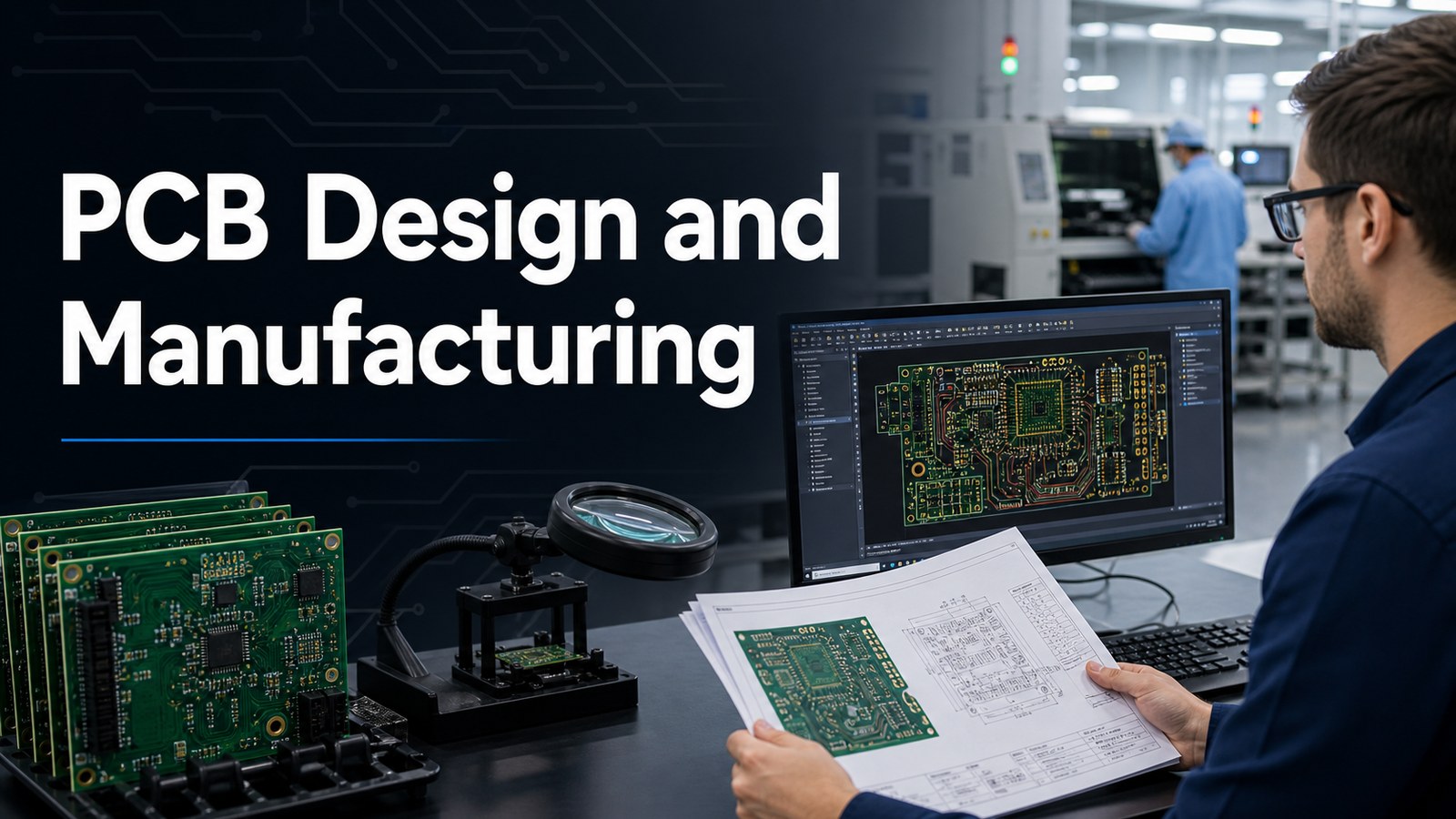
PCB design and manufacturing is the connected process of turning an electronic circuit idea into a manufacturable printed circuit board through schematic design, PCB layout, DFM review, fabrication, assembly and testing. A design is not truly finished until the manufacturer can build it with clear files, tolerances, materials and inspection requirements.
This guide is written for engineers, founders and buyers who need to move from design intent to a real PCB order. It follows the current search intent: definitions, design basics, manufacturing process, DFM mistakes, file preparation and RFQ handoff.
PCB Design and Manufacturing at a Glance
The best PCB projects connect design decisions with manufacturing constraints before files are released. Layout choices such as trace width, spacing, stackup, drill size, component placement and test access directly affect cost, yield and lead time.
| Stage | Main output | Manufacturing risk to control |
|---|---|---|
| Schematic | Circuit connectivity, power tree and interfaces | Missing design rules or test points. |
| Layout | Board outline, routing, planes and footprints | Clearance, assembly fit and signal integrity problems. |
| DFM review | Manufacturing comments and corrections | Unbuildable traces, holes, mask or panelization. |
| Fabrication | Bare PCB built from Gerber or ODB++ data | Wrong material, finish, thickness or drill assumptions. |
| Assembly | Components mounted and inspected | BOM, CPL, polarity and component sourcing errors. |
Is Your PCB Design Ready for Manufacturing Review?
PCB design and manufacturing problems often start before fabrication, when layout, footprints, BOM and test access are not checked together.
| Customer Pain Point | Project Risk | How bestpcbs Helps |
|---|---|---|
| Footprints or connector pinouts are wrong | The board may need a full redesign after the first build | bestpcbs encourages buyers to send complete fabrication and assembly files for DFM review before release. |
| Design rules do not match manufacturing constraints | Spacing, drill, annular ring or copper choices may cause delays | bestpcbs reviews Gerber or ODB++ files, drill data, copper and outline details during RFQ preparation. |
| Assembly and fabrication are reviewed separately | A board may fabricate correctly but create soldering or inspection problems | bestpcbs checks BOM, CPL and assembly notes together with board files when PCBA is required. |
| Testing access is planned too late | Debug and production checks become harder after layout is fixed | bestpcbs asks for test requirements and application constraints before production planning. |
What Is PCB Design and Manufacturing?
PCB design and manufacturing means designing the circuit board layout and then fabricating, assembling and testing the board so it can work as a physical product. Design answers what the board should do; manufacturing answers how it will be built reliably.
A complete project usually includes schematic capture, component selection, stackup planning, PCB layout, DFM review, Gerber or ODB++ export, drill files, BOM, CPL, assembly drawings, testing and revision control.
PCB Design and Manufacturing Buyer Priorities
PCB design and manufacturing should be connected before the quote stage, because layout decisions often decide fabrication cost, assembly risk and testing access. A buyer should not wait until production to discover spacing, drill, panelization or BOM conflicts.
Use supplier review to check board outline, stackup, copper, drill data, component placement, thermal constraints, assembly files and test access. This turns design handoff into a controlled manufacturing path instead of a file upload with unknown risks.
PCB Design Inputs Before Layout Starts
Good PCB manufacturing starts before layout, because the designer must know the board size, layer count, interfaces, power, current, signal speed, environment and assembly constraints. Missing inputs create redesign later.
- Electrical requirements: voltage, current, power and critical signals.
- Mechanical requirements: outline, mounting holes, connectors and enclosure limits.
- Manufacturing requirements: layer count, material, copper, finish and minimum features.
- Assembly requirements: component package, polarity, spacing and access for inspection.
- Testing requirements: test points, programming access and acceptance criteria.
Layout Decisions That Affect Manufacturing
PCB layout decisions affect whether the board can be fabricated, assembled, inspected and repeated without avoidable defects. A clean schematic can still become a difficult board if layout ignores manufacturing.
Check trace width, spacing, drill size, annular ring, solder mask bridge, copper-to-edge clearance, impedance needs, thermal relief, fiducials, polarity marks and panelization. The PCB design for manufacturability checklist is the most relevant internal guide for this stage.
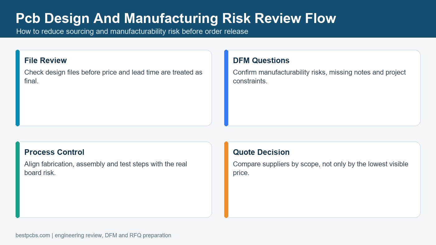
DFM Review Before PCB Fabrication
DFM review should happen before the PCB order is released because it catches manufacturing problems while they are still cheap to fix. It is the bridge between CAD output and factory reality.
DFM review can flag narrow copper, spacing conflicts, unsuitable drill sizes, missing solder mask clearance, incomplete board outline, unclear stackup and assembly access issues. For supplier selection, compare this with the PCB fabrication manufacturer guide.
PCB Manufacturing Process From Files to Boards
PCB manufacturing turns approved design files into bare boards through material preparation, imaging, etching, lamination if multilayer, drilling, plating, solder mask, silkscreen, surface finish, routing and testing. The exact route changes with board type and complexity.
Designers do not need to run every factory process, but they do need to understand which design choices affect them. Layer count, copper thickness, holes, slots, impedance and surface finish all change the manufacturing path.
PCB Assembly Data and Component Sourcing
PCB assembly requires more than bare-board files: it needs BOM, CPL, assembly drawings, component sourcing rules, polarity notes and inspection requirements. Many design-to-manufacturing delays happen at this handoff.
If you want turnkey PCBA, include PCBA and PCB assembly service requirements in the first quote. If parts need to be sourced, define approved alternates through component sourcing support before the order is committed.
Testing, Inspection and First Article Review
Testing and inspection should match the purpose of the first build: electrical continuity, assembly quality, firmware bring-up, power validation, thermal review or customer sample approval. A board that is not tested for the right question may still fail later.
For bare boards, electrical testing and visual inspection may be enough. For assembled boards, first article review, AOI, polarity checks, power-on checks or functional testing may be required.
Cost Factors in PCB Design and Manufacturing
PCB cost is driven by board size, layer count, material, copper, finish, drill density, feature limits, assembly scope, testing and urgency. Design choices made early often decide the final quote.
| Cost driver | Design decision behind it | How to control it |
|---|---|---|
| Layer count | Routing density, planes and signal needs | Choose the simplest stackup that meets performance. |
| Material | Temperature, signal, thermal and mechanical needs | Use special material only when the requirement is real. |
| Fine features | Trace, spacing, drill and BGA escape | Review DFM before release. |
| Assembly | BOM, package size, placement density and inspection | Provide clean BOM and CPL. |
Common Design-to-Manufacturing Mistakes
Common mistakes include treating layout as separate from manufacturing, exporting incomplete files, skipping DFM, delaying assembly data and changing revisions after quoting. These mistakes slow both prototypes and production.
- Sending Gerbers without drill files or stackup notes.
- Using footprints that do not match the real components.
- Forgetting test points, fiducials or polarity markings.
- Choosing a surface finish without considering assembly and storage.
- Requesting assembly before BOM and CPL are checked.
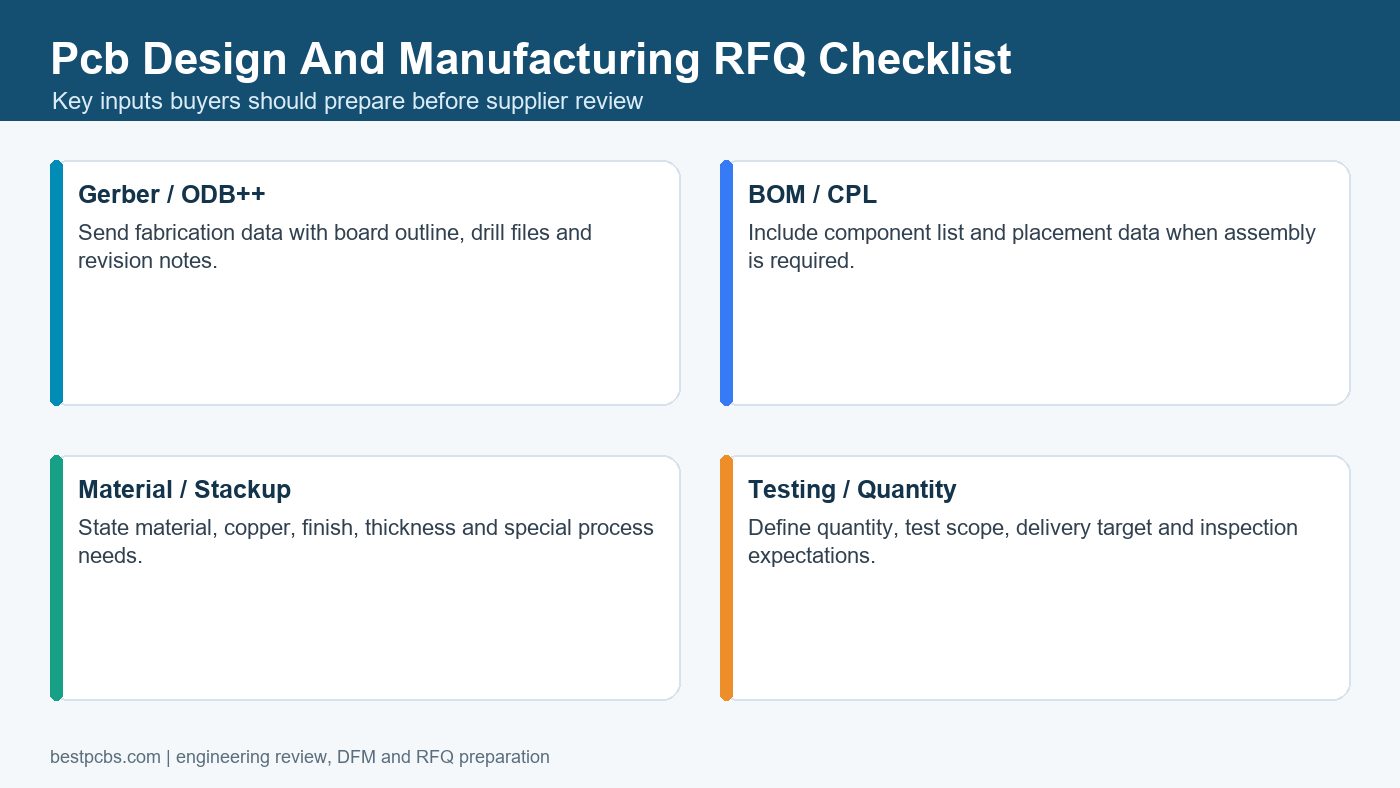
How to Prepare an RFQ Package
A good RFQ package lets the manufacturer quote the actual board, not a guessed version of it. This reduces back-and-forth and makes competing quotes easier to compare.
- Gerber or ODB++ files and drill files.
- Stackup, material, copper, finish and thickness requirements.
- Mechanical drawing for outline, slots and mounting holes.
- BOM, CPL and assembly drawing for PCBA.
- Testing and inspection requirements.
- Quantity, revision, target lead time and delivery destination.
Frequently Asked Questions About PCB Design and Manufacturing
What is PCB design and manufacturing?
PCB design and manufacturing is the process of designing a circuit board layout and then fabricating, assembling and testing it as a physical printed circuit board.
Is PCB manufacturing hard?
PCB manufacturing becomes difficult when the design has tight features, unclear files, unusual materials, dense assembly or missing test requirements. Good DFM review reduces that risk.
What files are needed for PCB manufacturing?
At minimum, manufacturers usually need Gerber or ODB++ files, drill files, stackup notes, board specifications and quantity. Assembly requires BOM, CPL and assembly drawings.
Can one supplier handle PCB design review and manufacturing?
Yes, many suppliers can review manufacturability and then fabricate or assemble the board. The key is to send complete design and production files.
Final RFQ Recommendation
Before moving from PCB design to manufacturing, check whether the design files, DFM assumptions, assembly data and testing plan describe the real board you want built. That is the difference between a CAD design and a manufacturable product.
For a PCB design and manufacturing review, send Gerber or ODB++ files, drill files, stackup, material and finish requirements, board drawings, quantity, BOM, CPL, assembly drawings, test requirements and target lead time to sales@bestpcbs.com. Best Technology / bestpcbs can review the package and help plan fabrication, assembly, component sourcing, prototype validation or production release.
You may also like



Tags: DFM Review, pcb design, pcb manufacturing