





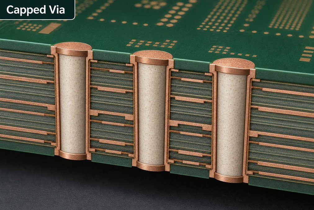
A capped via is a PCB via that is filled and then plated or capped over to create a sealed, flatter surface. It is often used when a via must be protected from solder wicking, contamination, voiding, or surface irregularity in dense PCB layouts.
For engineers and buyers, capped vias are not just a drawing detail. They affect manufacturability, inspection, cost, reliability, and how clearly the fabrication notes must be written before production.
What Is a Capped Via?
A capped via is a via hole that has been filled and then covered with copper plating or another specified cap structure.
In PCB manufacturing, vias connect copper layers through the board. A standard via may remain open, while a tented, plugged, filled, or capped via receives additional processing. A capped via usually provides a more protected surface than simple solder mask tenting, especially when the board has dense routing, fine-pitch parts, or via-in-pad requirements.
If you are comparing different via protection options, this related guide on tented via, filled via, and plugged via can help clarify the basic differences.
Why Are Capped Vias Used in PCB Manufacturing?
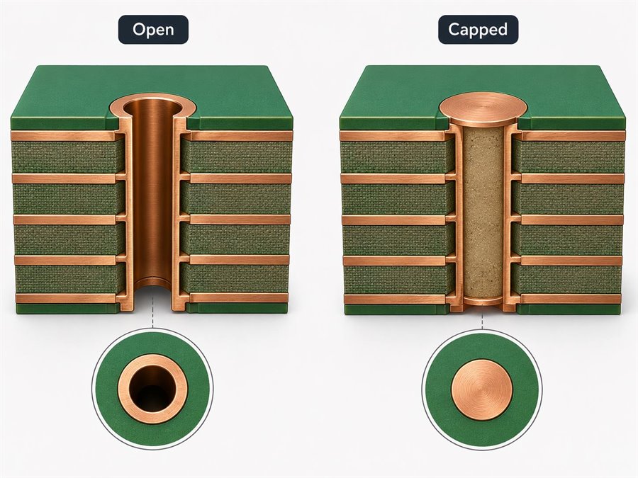
Capped vias are used to improve surface reliability, reduce solder-related problems, and support compact PCB layouts where ordinary open vias may create risk.
- They can help prevent solder from flowing into via holes during assembly.
- They can reduce contamination traps in exposed via openings.
- They can support smoother pad or surface areas when required by the layout.
- They can improve process control for high-density and reliability-focused PCB builds.
Capped vias are common in more complex products, including HDI PCB projects, dense BGA areas, compact control boards, and high-reliability electronics.
How Does the Capped Via Process Work?
The capped via process usually includes drilling, plating, filling, curing, planarization, cap plating, and inspection.
| Step | Purpose |
| Drilling | Create the via hole. |
| Plating | Form the conductive barrel. |
| Filling | Fill the via with specified material. |
| Curing | Stabilize the fill material. |
| Planarization | Flatten excess material. |
| Cap plating | Cover the filled via surface. |
| Inspection | Check filling, cap quality, and surface condition. |
For quality verification, a PCB cross section may be used to inspect via filling, plating, barrel condition, and cap structure when the project requires deeper validation.
What Is the Difference Between Filled and Capped Vias?
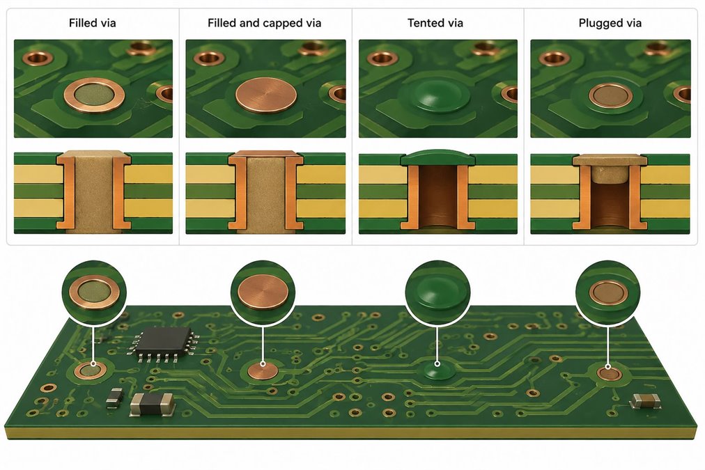
Filled vias focus on filling the hole, while capped vias add a covered surface after the via is filled.
| Via Type | Main Feature | Typical Use |
| Filled via | Via hole is filled. | Reduce voids or support reliability needs. |
| Filled and capped via | Filled via is covered by cap plating. | Improve surface condition and solder control. |
| Tented via | Solder mask covers the via opening. | Basic protection for suitable designs. |
| Plugged via | Via is plugged but not necessarily fully capped. | Cost-sensitive via protection. |
When Should You Choose Epoxy Filled and Capped Vias?
Epoxy filled and capped vias are useful when the via structure needs added protection, improved surface quality, or better assembly reliability.
This option may be considered for via-in-pad structures, BGA fanout areas, dense routing, boards with strict solderability needs, or applications where open via holes may create contamination or solder wicking concerns. The exact choice should be reviewed during DFM because cost and process complexity are higher than basic via tenting.
How Does IPC-4761 Type VII Define Filled and Capped Vias?
IPC-4761 Type VII is commonly referenced for filled and capped via structures, where the via is filled and then covered.
When a drawing or fabrication note calls out IPC-4761 Type VII filled and capped vias, the PCB supplier should understand the intended via protection level. Buyers should still confirm the exact fill material, plating expectation, acceptance criteria, inspection method, and whether the requirement applies to all vias or only selected vias.
Capped Via vs Via Capping: Are They the Same?
Capped via usually refers to the final via structure, while via capping refers to the process or requirement of covering a filled via.
In many engineering conversations, the terms overlap. However, fabrication notes should avoid vague wording. Instead of simply writing “cap vias,” it is better to specify whether the board needs filled and capped vias, which vias are included, whether IPC-4761 Type VII applies, and what inspection requirement is expected.
What PCB Design and Manufacturing Issues Can Capped Vias Help Prevent?
Capped vias can help reduce solder wicking, trapped residues, surface unevenness, and reliability concerns in dense PCB areas.
They are often discussed during PCB design for manufacturing review because the right via protection method depends on pad location, via size, solder mask strategy, surface finish, assembly process, and inspection needs.
For specialized boards that combine unusual material, thickness, copper, or via requirements, a special PCB manufacturing review can help confirm whether capped vias are appropriate.
How Should You Specify Capped Vias in PCB Fabrication Files?
Capped vias should be specified clearly in fabrication notes, stackup files, drill tables, and drawings so the supplier knows exactly which vias need the process.
- State whether the requirement is filled and capped via or another via covering type.
- Identify which via sizes or locations require capping.
- Call out IPC-4761 Type VII only when that is the intended structure.
- Define whether the requirement applies to via-in-pad areas, BGA areas, or all vias.
- Confirm inspection expectations before production.
If the instruction is unclear, the supplier may quote the wrong process or ask for clarification, which can delay the project.
FAQs about Capped Via
Is a capped via the same as a filled via?
No. A filled via means the hole is filled. A capped via normally means the filled via is also covered by a cap or plating layer.
Is via capping always required for via-in-pad?
Not always, but via-in-pad designs often require filled and capped vias to prevent solder loss and surface problems during assembly.
Does IPC-4761 Type VII mean filled and capped vias?
Yes, IPC-4761 Type VII is commonly used to describe filled and capped via protection. The exact fabrication note should still be reviewed with the PCB supplier.
Are capped vias more expensive?
Yes. Capped vias add filling, curing, planarization, plating, and inspection steps, so they usually cost more than standard open or tented vias.
What should I send for a capped via quote?
Send Gerber or ODB++ files, drill files, stackup, via table, fabrication notes, IPC requirement, surface finish, quantity, lead time, and inspection expectations.
In Conclusion, a capped via can improve PCB manufacturability and assembly reliability when the board needs protected, filled, and plated via structures. To avoid quotation mistakes, specify the via type clearly, review IPC-4761 Type VII requirements carefully, and confirm the process with your PCB manufacturer before production.
EBest Circuit (Best Technology) supports PCB manufacturing, DFM review, PCB layout manufacturability review, component sourcing, PCBA assembly, and testing support. If you need help reviewing capped via requirements for a PCB or PCBA project, contact the engineering team at sales@bestpcbs.com.
You may also like






Tags: capped via, filled vias, IPC-4761, PCB via