

GPS Antenna PCB is a specialized printed circuit structure designed to receive satellite signals and convert them into stable positioning data for devices such as trackers, automotive systems, IoT modules, and industrial equipment. This article explains how GPS antenna PCB design, material selection, frequency planning, assembly control, and testing work together when choosing a reliable manufacturer for fast prototyping, design, and assembly.
Are you struggling with unstable signal performance, repeated antenna tuning, or unclear supplier capabilities when sourcing a gps antenna pcb manufacturer?
- The prototype performs well in lab conditions but fails in the final product
- Antenna matching shifts after PCB fabrication
- GPS signal becomes weak after enclosure integration
- Supplier lacks RF understanding beyond PCB fabrication
- Quotation and engineering response are slow
These issues often come from a disconnect between design, material selection, and manufacturing execution.
- Align antenna design with real product structure from the beginning
- Select materials based on RF behavior, not just cost
- Control PCB fabrication tolerances for RF consistency
- Integrate layout, assembly, and testing as one process
- Provide fast engineering feedback and prototyping support
EBest Circuit (Best Technology) is a professional PCB and PCBA manufacturer with strong experience in RF-related products. We support gps antenna pcb design, gps antenna pcb layout, and full assembly services, helping customers move efficiently from concept to mass production. Ready to move your GPS antenna PCB project forward? Contact our team at sales@bestpcbs.com for fast engineering support and manufacturing solutions.
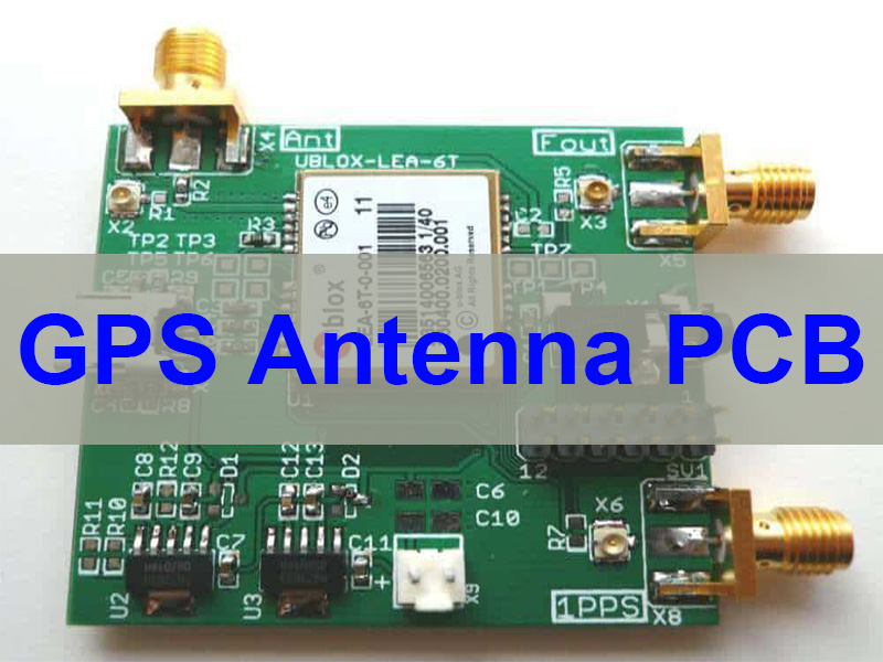
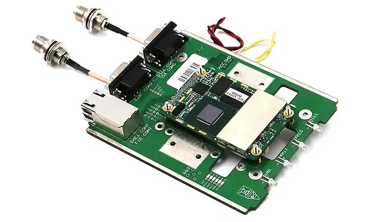
What Is a GPS Antenna PCB?
A GPS antenna PCB is not simply a circuit board carrying a GNSS module. In many modern designs, the antenna itself is implemented directly on the PCB or integrated into it as part of the RF structure.
From an engineering perspective, a gps antenna on pcb must handle extremely weak satellite signals while operating inside complex electronic environments. This includes interference from processors, power circuits, shielding, and enclosure materials.
Key structural elements
- Radiating element (patch or trace)
- RF feed line
- Ground plane
- Matching network
- Optional LNA (for active designs)
| Element | Role |
|---|---|
| Antenna | Receives satellite signal |
| Feed line | Transfers RF signal |
| Ground plane | Stabilizes performance |
| Matching network | Ensures impedance matching |
| LNA | Amplifies weak signals |
In essence, a GPS antenna PCB behaves more like an RF component than a conventional PCB, which is why manufacturing precision directly impacts performance.
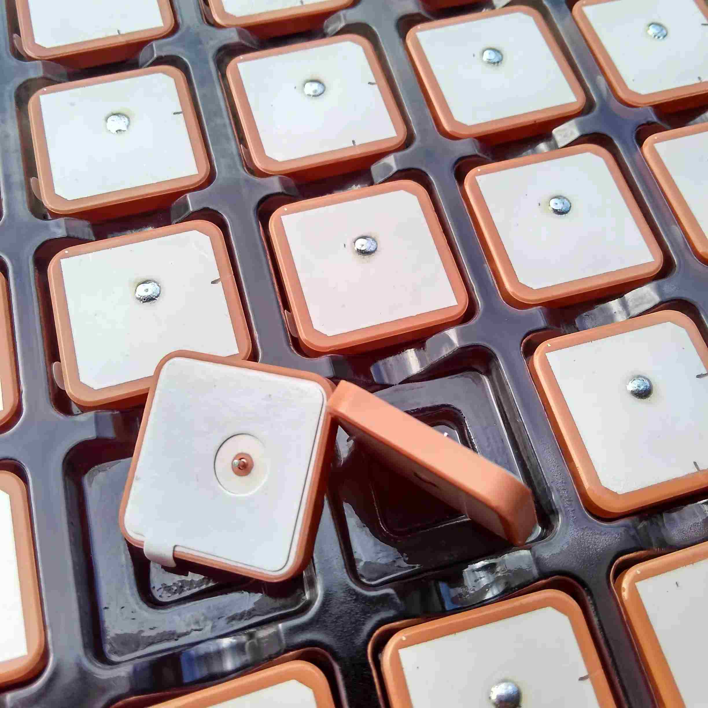
What Are the Main Types of GPS PCB Antennas? (Patch vs Trace vs Active)
When selecting a gps pcb antenna, engineers are not just choosing a structure—they are defining how the antenna interacts with the entire system.
Main antenna types
- Patch antenna
Provides stable performance and is widely used in navigation systems. - PCB trace antenna
A gps PCB trace antenna is etched directly on the board, reducing cost but increasing sensitivity to layout conditions. - Active antenna
An active gps antenna pcb includes an amplifier to improve signal strength in weak environments. - Flexible antenna
A flexible pcb gps antenna allows placement flexibility in compact devices. - GPS + Cellular antenna
A gsm gps pcb antenna integrates positioning and communication but requires careful isolation.
| Type | Advantage | Limitation |
|---|---|---|
| Patch | Stable performance | Needs ground plane |
| Trace | Low cost | Easily detuned |
| Active | High sensitivity | More complex |
| Flex | Flexible placement | Sensitive to structure |
| Combo | Space saving | RF interference risk |
The choice depends on product size, signal requirements, and integration complexity.
What Materials Are Used in Flexible PCB GPS Antennas?
Flexible GPS antennas typically use polyimide substrates, allowing the antenna to be positioned away from interference sources.
However, material selection is not just about flexibility. It directly affects signal stability, loss, and repeatability.
Material comparison
| Material | Use Case | Advantage | Limitation |
|---|---|---|---|
| FR4 | Standard designs | Low cost | Higher RF loss |
| RF materials | High-performance designs | Stable dielectric | Higher cost |
| Flex (Polyimide) | Compact devices | Flexible placement | Harder tuning |
In real-world projects:
- FR4 is widely used for cost-sensitive designs
- RF materials are chosen for performance-critical applications
- Flex is selected when mechanical constraints dominate
The best material is always determined by system-level requirements, not just electrical specifications.
How to Design a GPS Patch Antenna PCB?
A gps patch antenna pcb design begins with frequency selection, ground plane definition, and system constraints.
Design process
- Define operating frequency
- Select antenna structure
- Estimate dimensions based on wavelength
- Ensure continuous ground plane
- Control RF feed impedance
- Reserve matching network area
- Validate through testing
Key layout rules
- Keep RF area isolated from digital noise
- Avoid ground discontinuities
- Minimize feed length
- Maintain symmetry
- Allow tuning flexibility
A well-designed antenna depends more on layout discipline than theoretical complexity.
What Frequency Bands Do GPS PCB Antennas Operate In? (L1 / L2 / L5)
GPS antenna PCB design is based on L-band frequencies, but different applications may require different frequency combinations.
Main frequency bands
| Band | Frequency | Typical Use |
|---|---|---|
| L1 | 1575.42 MHz | Standard GPS |
| L2 | 1227.60 MHz | Dual-frequency |
| L5 | 1176.45 MHz | High reliability |
In most commercial designs, L1 remains the primary target. However, advanced applications may use multiple bands to improve positioning accuracy.
For gps glonass pcb antenna or multi-constellation systems, bandwidth requirements increase, making design more complex.
The key point is that frequency selection defines antenna size, material choice, and matching strategy.
How to Calculate GPS Antenna Wavelength and Patch Size?
A fundamental step in antenna design is calculating wavelength.

For L1 frequency:

However, real antenna size depends on the effective dielectric constant:
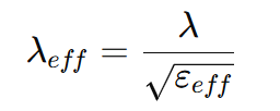
Practical design steps
- Calculate free-space wavelength
- Adjust for substrate properties
- Determine initial patch size
- Optimize through testing
Actual dimensions are influenced by:
- Substrate thickness
- Ground plane size
- Feed position
- Enclosure effects
So calculations provide a starting point, but tuning is always required.
What Are the Challenges in GPS Antenna PCB Assembly?
Assembly plays a critical role in antenna performance.
Common challenges
- Placement misalignment
- Solder thickness variation
- Board warpage
- Shield interference
- Cable coupling
For active pcb gps antenna, these issues become more critical due to amplification effects.
| Factor | Impact |
|---|---|
| Placement | Frequency shift |
| Solder | Impedance change |
| Ground | Signal instability |
| Shielding | Radiation distortion |
Assembly must be treated as part of RF design, not a separate process.
Top 10 GPS PCB Antenna Design Factories in China
Below is a practical reference list of companies active in GPS antenna and RF PCB manufacturing:
| Company | Positioning |
|---|---|
| EBest Circuit | PCB + PCBA + RF support |
| C&T RF Antennas | Custom antenna design |
| JC Antenna | GNSS antenna specialist |
| Tengxiang Electronics | RF components manufacturer |
| Signal Plus | GPS antenna supplier |
| NHAIT | Custom FPC antenna |
| Keesun Technology | Embedded antenna provider |
| Chang Hong | GNSS antenna supplier |
| Leheng Electronics | GPS antenna solutions |
| Bynav ecosystem | GNSS system providers |
Choosing a supplier should focus on engineering capability, not just production capacity.
What Are the Applications of GSM GPS PCB Antennas?
A gsm gps pcb antenna is widely used in connected devices.
Typical applications
- Vehicle tracking
- Fleet management
- IoT devices
- Smart meters
- Security systems
- Wearables
These applications require both positioning and communication, making integrated antenna solutions essential. Pls feel free to reach out to our engineering team at sales@bestpcbs.com for fast support and reliable solutions.
How to Test GPS Antenna PCB Performance? (Gain / Return Loss)
Testing ensures real-world performance.
Key parameters
- Return loss (S11)
- Gain
Practical validation steps
- Measure return loss
- Verify frequency alignment
- Test signal reception
- Evaluate in final enclosure
- Compare multiple samples
A common mistake is testing only on a bare PCB. Final product testing is essential.
How to Get GPS PCB Antenna Quotes from EBest Circuit (Best Technology)?
To get accurate gps pcb antenna quotes, prepare:
- Gerber files
- Frequency requirements
- Material preference
- Board dimensions
- Assembly requirements
- Quantity
To summarize, GPS Antenna PCB is a critical RF structure that determines positioning accuracy and signal reliability in modern electronic devices. This article covered antenna types, materials, design methods, frequency bands, calculations, assembly challenges, and testing processes.
EBest Circuit (Best Technology) provides complete support from design review to PCB fabrication and PCBA assembly, ensuring faster development and more reliable RF performance. Pls feel free to send your files to sales@bestpcbs.com for fast evaluation and quotation.
FAQs About GPS Antenna PCBs
1. What is the most common GPS antenna type?
Patch antennas are widely used due to stable performance.
2. Can FR4 be used?
Yes, but performance may vary compared to RF materials.
3. Why does performance change after assembly?
Because enclosure and components affect RF behavior.
4. What is an active antenna?
An antenna with an integrated amplifier.
5. Can GPS and cellular share one PCB?
Yes, but requires careful RF design.
You may also like

Tags: active gps antenna pcb, GPS Antenna PCB, gps antenna pcb layout, gps patch antenna pcb design, gps pcb antenna, gps pcb antenna design