

In power-dense electronics, standard PCB construction often becomes the limiting factor rather than the circuit design itself. Excessive temperature rise, copper fatigue, and current bottlenecks are common failure modes once current levels move beyond conventional ranges. This is where a reliable heavy copper PCB manufacturer stands out. Heavy copper PCBs are engineered specifically to handle high current, elevated thermal loads, and demanding mechanical stress while maintaining long-term reliability.
At Best Technology, we specialize in manufacturing premium heavy copper PCBs that meet and exceed IPC-A-610 requirements, tailored to the unique needs of high-power electronics. In this blog, we’ll break down everything you need to know about heavy copper PCBs—from what defines them to how to choose the right manufacturer, plus real-world case studies and answers to your most pressing questions.
What Makes a PCB “Heavy Copper”?
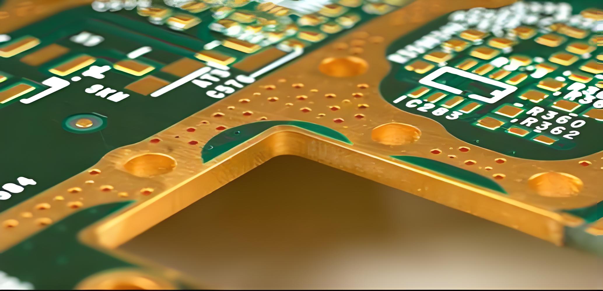
A PCB is typically classified as heavy copper when the finished copper thickness on one or more layers exceeds 3 oz/ft² (≈105 µm). Many industrial designs extend well beyond this threshold, reaching 6 oz, 10 oz, or even 20 oz copper, depending on current and thermal requirements.
Unlike standard boards, heavy copper PCBs are not simply “thicker copper versions” of conventional designs. They require dedicated imaging, etching, plating, and lamination strategies to maintain conductor geometry, dielectric integrity, and layer-to-layer registration.
Why Heavy Copper Matters in High-Power Electronics?
As power electronics continue to shrink in size, current density inevitably increases. Heavy copper construction directly addresses this challenge by offering:
- Higher current-carrying capacity without excessive temperature rise
- Lower conductor resistance, improving energy efficiency
- Improved thermal spreading, reducing hot spots
- Enhanced mechanical strength, especially around plated through holes and power vias
In applications such as EV power modules, industrial motor drives, and renewable energy converters, heavy copper is often the difference between theoretical performance and field reliability.
Technical Specifications: Copper Weight & Conductivity
Copper thickness is usually specified in ounces per square foot, but its real impact is seen in electrical and thermal performance.
Typical heavy copper parameters include:
- Copper thickness: 3 oz to 20+ oz (105 µm to >700 µm)
- Trace current capacity: Several times higher than 1-oz copper at equivalent temperature rise
- Lower voltage drop: Especially critical for low-voltage, high-current systems
- Thermal conductivity: Copper’s intrinsic conductivity enables efficient heat spreading across planes and embedded power structures
A qualified heavy copper PCB manufacturer will validate these parameters against IPC guidelines rather than relying on theoretical calculations alone.
Heavy Copper PCB Manufacturing Challenges
Manufacturing heavy copper PCBs is more complex than standard ones, requiring specialized equipment and strict quality control. Key challenges we address at Best Technology:
- Etching Uniformity: Thicker copper is hard to etch evenly, causing uneven traces or undercutting. We use controlled depth etching and precision equipment for consistent, clean traces.
- Plating Consistency: Multilayer PCBs need thick, uniform via plating. Our optimized electroplating ensures reliable via connections, avoiding high resistance or thermal failure.
- Thermal Stress: Copper and substrates (e.g., FR-4) expand differently under heat, causing warping or delamination. We use temperature-controlled lamination to minimize stress.
- IPC-A-610 Compliance: Meeting this standard (trace geometry, plating, solder joints) requires rigorous quality control at every manufacturing stage.
Design Guidelines for Heavy Copper PCB
Heavy copper PCB design should follow one core principle: current-driven, precisely matched copper. Simply increasing copper thickness often raises cost and introduces new risks, including uneven heat dissipation, soldering difficulty, and mechanical stress. Effective heavy copper design balances electrical demand with manufacturability.
1. Copper Thickness Selection
Choose copper thickness based on actual current, not excessive margin.
Formula (ambient ≤ 40 °C):
Allowable current (A) ≈ Copper thickness (oz) × Trace width (mm) × 0.8
For example:
3 oz copper × 3 mm trace ≈ 7.2 A, suitable for most industrial power designs.
Recommendations:
- Prefer 3–6 oz, which covers most applications
- Above 10 oz increases risks of warpage and drilling difficulty
- Avoid overdesign unless required by aerospace or defense systems
2. Trace Design for High Current
Trace geometry must support smooth current flow.
- 3 oz copper: minimum trace width ≥ 0.3 mm
- 6 oz copper at 10 A: recommended width ≥ 5 mm
Avoid sudden width changes. Use gradual tapers (length ≥ 3× width difference) to prevent current crowding and localized heating.
For thermal control, use copper pours under power devices combined with thermal vias (Ø 0.8–1.2 mm, pitch 2–3 mm) to transfer heat into internal planes.
3. Via Design Considerations
Vias are a critical limitation point in heavy copper PCBs.
- Minimum finished hole ≥ 0.8 mm (3 oz copper)
- Via wall copper ≥ 20 µm
Do not rely on a single via for high current. A 5 A path on 3 oz copper typically requires 2–3 parallel vias, as one via carries only 2–3 A reliably.
Ensure adequate solder mask opening (hole + 0.2–0.3 mm) to prevent solder blockage.
4. Stack-Up and Material Selection
Place heavy copper layers on outer or near-outer layers and keep copper distribution symmetrical to prevent warpage.
Select high-Tg materials (Tg ≥ 170 °C), such as FR-4 Tg170 or polyimide, to withstand higher thermal load during assembly and operation.
5. Assembly Adaptation
Heavy copper absorbs more heat during soldering.
- Use large power packages (e.g., TO-220, D2PAK)
- Enlarge pads by 0.2–0.3 mm compared to standard designs
- Increase reflow peak temperature by 5–10 °C and extend soak time by 10–15 s to avoid cold solder joints
Top Industries Using Heavy Copper PCBs
Heavy copper PCBs are widely used in industries that demand power, durability, and reliability:
- Power supplies & converters
- Electric vehicles (EV) & charging systems
- Industrial motor drives
- Renewable energy (solar, wind, inverters)
- Aerospace & defense electronics
- Medical imaging and power modules
These industries rely on certified heavy copper PCB manufacturers to meet strict quality standards.
How to Choose a Heavy Copper PCB Manufacturer?
Choosing the right heavy copper PCB manufacturer is a strategic decision that directly affects product quality and lifecycle cost.
Important evaluation criteria include:
- Proven experience with multi-ounce copper designs
- Clear alignment with IPC-A-610 and IPC-6012 standards
- Robust process control and inspection capability
- Engineering support for DFM and design optimization
- Ability to scale from prototype to volume production
Manufacturers that lack dedicated heavy copper expertise often struggle with yield, consistency, and long-term reliability.
Why Choose Best Technology as Your Heavy Copper PCB Manufacturer?
With over 20 years of experience in heavy copper PCB manufacturing, Best Technology has the expertise to handle even the most complex projects—from standard heavy copper (3 oz – 5 oz) to extra-thick copper (up to 20 oz). Our team of engineers specializes in solving the unique challenges of heavy copper PCB design and manufacturing.
We offer fully customized heavy copper PCBs to meet your project’s unique requirements. Whether you need a specific copper weight, substrate, surface finish, or board size, we can tailor our solutions to fit your needs.
We deeply know the importance of quality for every product, so we ensure the full traceability from design, manufacturing to shipment. We strictly adhere to IPC-A-610 standards (Class 2 and Class 3) for every heavy copper PCB we manufacture. In addition to this, due to heavy copper PCB always used in electric vehicles, our facility obtained the IATF16949 and AS9100D certifications to ensure each process are under rigorous control.
Heavy Copper PCB Case Studies in Best Technology
Case Study 1: EV Battery Management System (BMS) PCB
Customer: A leading global automotive manufacturer specializing in electric vehicles.
Challenge: The customer needed a heavy copper PCB for their EV BMS that could handle high currents (up to 200A), dissipate heat efficiently, and meet IPC-A-610 Class 3 standards. The PCB also needed to be compact to fit within the EV’s battery pack.
Solution: We designed and manufactured a 6 oz heavy copper PCB using high-temperature FR-4 substrate and ENIG surface finish. We integrated copper pours and thermal vias to improve thermal management, and optimized the trace width and spacing to handle the high current load. We also used blind vias to save space, ensuring the PCB fit within the customer’s compact design.
Result: The PCB met all IPC-A-610 Class 3 requirements, handled the 200A current load without overheating, and reduced the BMS’s overall size by 15%. The customer has since expanded their partnership with us for all their EV BMS PCB needs.
Case Study 2: Solar Inverter PCB
Customer: A renewable energy company specializing in solar inverters.
Challenge: The customer needed a heavy copper PCB for their 50kW solar inverter that could handle high voltages (up to 1000V) and dissipate heat in outdoor environments. The PCB also needed to be durable enough to withstand extreme temperature fluctuations (-40°C to 85°C).
Solution: We manufactured a 10 oz heavy copper PCB using polyimide substrate (for high-temperature resistance) and immersion silver surface finish (for excellent conductivity). We designed the PCB with wide traces (0.030 inches) to handle the high voltage and current, and integrated large copper pours to dissipate heat. We also used a conformal coating to protect the PCB from outdoor elements.
Result: The PCB operated reliably in extreme temperature conditions, handled the 1000V voltage load without failure, and reduced the inverter’s heat-related downtime by 80%. The customer reported a 20% increase in inverter efficiency due to the PCB’s superior thermal management.
Our Heavy Copper PCB Manufacturing Capabilities
At Best Technology, we have the capabilities to handle all your heavy copper PCB needs—from prototype to production. Here’s a breakdown of our key manufacturing capabilities:
- Base Material: FR4/Aluminum
- Copper Weight: 3 oz – 20 oz (105 μm – 700 μm) for single-sided, double-sided, and multilayer PCBs.
- Extreme Heavy Copper: 20-200OZ
- Outline: Routing, punching, V-cut
- Layer Count: 1 layer – 40 layers (multilayer heavy copper PCBs with blind/buried vias available).
- Surface Finishes: HASL, ENIG, OSP, Immersion gold
- Solder Mask: White, Black, Blue, Green, Red
- Tolerances: Trace width tolerance ±0.001 inches, copper thickness tolerance ±10%, board thickness tolerance ±0.005 inches.
- Board Size: Up to 24 inches x 36 inches (609.6 mm x 914.4 mm), with custom sizes available.
- Quality Control: X-ray inspection, optical inspection (AOI), flying probe testing, thermal cycling testing, and IPC-A-610 compliance testing.
- Production Capacity: Prototype runs (1 – 100 units), small batch production (100 – 1000 units), and large-scale production (1000+ units) with lead times as short as 3 days for prototypes.
- Support for prototypes, small batches, and stable mass production
FAQs About Heavy Copper PCBs
1. When should I choose a heavy copper PCB over a standard PCB?
Choose a heavy copper PCB if your project requires:
- High current carrying capacity (more than 10A).
- Enhanced thermal management (e.g., applications operating at high temperatures or generating significant heat).
- Greater mechanical strength (e.g., rugged industrial or automotive applications).
- Reduced component count (replacing discrete heat sinks or bus bars).
Standard PCBs are sufficient for low-power applications (e.g., consumer electronics with low current demands).
2. How is heavy copper PCB manufacturing different from standard PCB manufacturing?
Heavy copper PCB manufacturing requires specialized processes to handle the thicker copper layers, including:
- Controlled depth etching to ensure uniform trace widths and clean edges.
- Optimized electroplating processes to ensure consistent via plating thickness.
- Temperature-controlled lamination to minimize thermal stress and prevent warping/delamination.
- Rigorous quality control to meet IPC-A-610 standards, including X-ray inspection for via integrity.
Standard PCB manufacturing uses simpler etching and plating processes, as the thinner copper layers are easier to handle.
3. Are heavy copper PCBs more expensive?
Yes, heavy copper PCBs are typically more expensive than standard PCBs. The higher cost is due to:
- More copper material (thicker layers require more copper).
- Specialized manufacturing processes (e.g., controlled etching, optimized plating).
- Rigorous quality control (e.g., X-ray inspection, thermal testing).
However, the extra cost is often offset by the benefits: reduced component count, longer lifespan, improved reliability, and lower maintenance costs. For high-power applications, heavy copper PCBs are a cost-effective long-term investment.
4. How does copper thickness influence current carrying capacity?
Copper thickness has a direct impact on current carrying capacity: thicker copper layers have lower electrical resistance, allowing them to carry more current without overheating. As a general rule, the current carrying capacity of a copper trace increases linearly with copper thickness. For example:
- 1 oz copper trace (35 μm): ~5A current carrying capacity (at 25°C temperature rise).
- 3 oz copper trace (105 μm): ~15A current carrying capacity (at 25°C temperature rise).
- 10 oz copper trace (350 μm): ~50A current carrying capacity (at 25°C temperature rise).
A reputable heavy copper PCB manufacturer will help you select the right copper thickness based on your project’s current requirements and thermal constraints.
5. Can heavy copper PCBs be multilayered?
Yes, heavy copper PCBs can be multilayered. Multilayer heavy copper PCBs are used in high-power applications that require both high current carrying capacity and complex circuitry (e.g., EV BMS, solar inverters, aerospace systems). We specialize in manufacturing multilayer heavy copper PCBs with up to 40 layers, including blind and buried vias to save space and improve signal integrity.
6. How to avoid heat-related failures in heavy copper PCBs?
To avoid heat-related failures, follow these best practices:
- Use thick copper layers (3 oz or more) to dissipate heat efficiently.
- Integrate thermal management features like copper pours, thermal vias, and heat sinks.
- Choose a high-temperature substrate (e.g., polyimide) for applications operating at extreme temperatures.
- Optimize trace design (wider traces) to reduce resistance and heat generation.
- Work with a heavy copper PCB manufacturer that adheres to IPC-A-610 standards, ensuring proper plating and trace integrity.
Ready to Start Your Heavy Copper PCB Project?
If you’re working on a high-power electronics project that requires premium heavy copper PCBs—ones that meet IPC-A-610 standards, deliver superior performance, and fit your budget—look no further than Best Technology. As a trusted heavy copper PCB manufacturer with over 20 years of experience, we have the expertise, equipment, and dedication to bring your project to life.
Here’s how to get started:
1. Share Your Requirements: Send us your PCB design files, copper weight needs, substrate preferences, and application details.
2. Get a Custom Quote: Our team will review your requirements and provide a competitive, no-obligation quote within 24 hours.
3. Design Support (If Needed): Our engineers will work with you to optimize your design for performance, manufacturability, and cost.
4. Manufacturing & Delivery: We’ll manufacture your heavy copper PCBs to IPC-A-610 standards, conduct rigorous quality control, and deliver them on time—whether you need prototypes or large-scale production.
Don’t settle for subpar heavy copper PCBs that put your project at risk. Choose Best Technology—the premium heavy copper PCB manufacturer that delivers reliability, performance, and peace of mind. Contact us today to discuss your heavy copper PCB project!
You may also like


Tags: heavy copper pcb, heavy copper pcb design, Heavy copper PCB manufacturer