Wave soldering is one of the most established and reliable PCB assembly methods used in electronics manufacturing. Although surface mount technology (SMT) and reflow soldering dominate modern production, wave soldering PCB processes remain essential for through-hole components, mixed-technology boards, and high-reliability applications.
In this guide, we’ll explain what wave soldering is, how it works, its benefits and requirements, and clearly compare wave soldering vs reflow to help you choose the right process for your project.
What Is Wave Soldering?
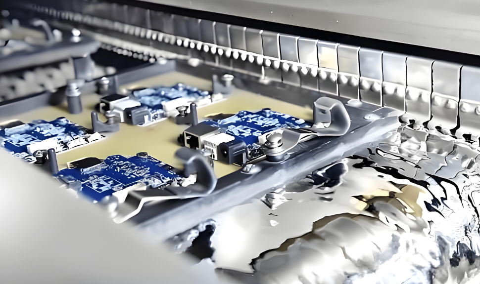
Wave soldering is a mass soldering process in which the underside of a populated printed circuit board passes over one or more controlled waves of molten solder. The solder wets the exposed pads and component leads, forming metallurgical bonds in a single pass.
This process is primarily used for:
- Through-hole components
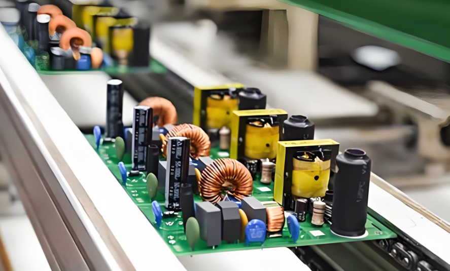
- Large connectors and terminals
- Power components
- Mixed-technology (SMT + THT) assemblies
Wave soldering PCB assembly is widely applied in industrial electronics, automotive systems, power supplies, aerospace hardware, and medical equipment, where joint integrity and mechanical strength are critical.
What is Wave Soldering? Wave soldering vs Reflow Soldering
Benefits of Wave Soldering
Although newer soldering technologies exist, wave soldering continues to offer clear advantages for specific applications.
- High Throughput for Through-Hole Assembly
- Superior Mechanical Strength
- Process Stability and Repeatability
- Cost Efficiency in Volume Production
- Compatibility with Mixed-Technology Designs
How Does Wave Soldering Work?
The wave soldering process is a tightly controlled sequence of thermal and chemical stages. Each stage must be optimized to ensure solder joint integrity and prevent defects.
1. Flux Application
Flux is applied to the bottom side of the PCB by spray, foam, or jet fluxing. Its function is to:
- Remove oxides from pads and leads
- Improve solder wetting
- Prevent oxidation during heating
Proper flux selection and coverage are critical to avoiding non-wetting and bridging defects.
2. Preheating
The PCB is gradually heated using infrared or convection heaters. Preheating:
- Activates the flux
- Drives off solvents
- Reduces thermal shock to components
- Improves solder flow and hole fill
Inadequate preheat is a common root cause of soldering defects.
3. Solder Wave Contact
The board passes over one or more solder waves:
- Turbulent wave for penetration around component leads
- Laminar wave for smoothing and joint shaping
The molten solder wets the pads and leads through capillary action, forming intermetallic bonds.
4. Cooling and Solidification
After leaving the wave, the assembly is cooled in a controlled manner to solidify the solder joints and stabilize the microstructure.
Is Wave Soldering the Most Common Soldering Method?
No. Reflow soldering is the dominant process in modern electronics manufacturing due to the prevalence of SMT components and high-density designs.
However, wave soldering remains:
- The primary method for through-hole assembly
- Essential for power electronics and connector-heavy designs
- Common in automotive, industrial control, and infrastructure equipment
In many products, both processes are used in sequence: reflow for SMT components, followed by wave soldering for through-hole parts.
What Temperature Is Wave Soldering?
Wave soldering temperature depends on the solder alloy:
- Lead-free solder (SAC alloys): 245°C – 260°C
- Leaded solder (SnPb): 230°C – 250°C
Temperature control is critical:
- Excessive temperature can cause delamination, pad lifting, and component damage
- Insufficient temperature leads to poor wetting, cold joints, and incomplete hole fill
A properly developed thermal profile is mandatory for high-reliability wave soldering PCB assembly.
What Is the Minimum Pitch for Wave Soldering?
Wave soldering is not suitable for fine-pitch components. Typical design limits are:
- Recommended minimum pitch: 2.5 mm (0.1”)
- Below 2.0 mm, it will occur potential risk like:
- Solder bridging
- Incomplete solder fill
- Shorts between adjacent pins
For fine-pitch or high-density layouts, reflow soldering or selective soldering is the preferred solution.
Wave Soldering Requirements
Successful wave soldering depends on coordinated control of design, materials, and process parameters.
PCB Design Requirements
- Adequate pad size and annular ring
- Proper hole-to-lead diameter ratio
- Solder mask dams to control solder flow
- Component orientation aligned with solder wave direction
Component Requirements
- Leads compatible with wave soldering temperatures
- Suitable lead finishes (Sn, SnCu, NiAu)
- Proper lead protrusion for reliable hole fill
Process Control Requirements
- Stable solder pot temperature
- Controlled conveyor speed and immersion time
- Consistent flux density and application
- Clean solder alloy with minimal dross
Ignoring any of these requirements significantly increases defect risk.
What Is the Difference Between Reflow and Wave Soldering?
| Parameter | Wave Soldering | Reflow Soldering |
| Primary Application | Through-hole components | Surface mount components |
| Solder Application | Molten solder wave | Solder paste + thermal reflow |
| Component Density | Low to medium | High to ultra-high |
| Pitch Capability | ≥ 2.5 mm | Down to 0.3 mm |
| Mechanical Strength | Very high | Moderate |
| Design Flexibility | Limited | Excellent |
| Typical Use | Connectors, power parts | ICs, BGAs, QFNs, passives |
Key Engineering Differences
- Wave soldering PCB assembly excels in mechanical robustness and hole fill quality
- Reflow soldering supports miniaturization, fine pitch, and high component density
- Many assemblies require both processes to meet functional and mechanical requirements
The decision between wave soldering vs reflow should be made during the DFM stage, not after layout completion.
What Is the Alternative to Wave Soldering?
When wave soldering is not suitable, alternatives include:
Selective Soldering
- Computer-controlled mini-wave solders specific joints only
- Ideal for mixed-technology assemblies
- Reduces risk to nearby SMT components
Pin-in-Paste (Intrusive Reflow)
- Through-hole leads are inserted into solder paste and reflowed
- Suitable for low-profile connectors and moderate volumes
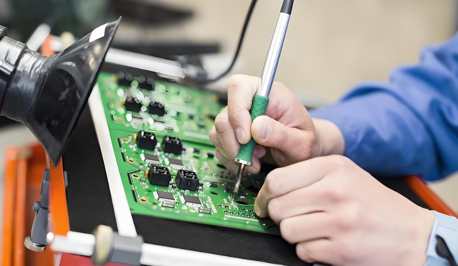
Hand Soldering
- Used for prototypes, rework, and very low volumes
- Highly flexible but labor intensive and variable
Each alternative has trade-offs in cost, throughput, and reliability.
When Should You Use Wave Soldering PCB Assembly?
Wave soldering is the correct choice when:
- Your design includes large through-hole connectors or terminals
- Mechanical strength and vibration resistance are critical
- You are producing medium to high volumes
- Long-term reliability outweighs miniaturization
For power electronics, industrial controllers, and infrastructure equipment, wave soldering remains the industry standard.
Why Choose EBest Circuit (Best Technology) for Wave Soldering PCB Assembly?
At EBest Circuit (Best Technology), wave soldering is treated as a controlled engineering process—not a commodity operation. We apply strict process discipline, DFM analysis, and IPC-compliant inspection to every project.
Our Capabilities Include:
- Leaded and lead-free wave soldering
- Mixed technology (SMT + THT) assemblies
- Selective soldering for complex designs
- IPC-A-610 compliant inspection
- Full DFM review before production
Our manufacturing system operates under ISO 13485 quality management controls, ensuring traceability, documentation, and process consistency—even without a fully isolated medical production line. Contact EBest Circuit (Best Technology) today to request a free DFM review and quote for your wave soldering PCB assembly project.
You may also like


Tags: wave soldering, Wave soldering pcb, Wave soldering vs reflow