The SMT PNP process is the core stage in surface mount technology where electronic components are precisely placed onto a PCB, determining the assembly’s accuracy, reliability, and performance. This article provides a detailed explanation of the SMT pick-and-place process—from its definition and operational steps to key optimization methods—helping engineers and manufacturers achieve high-yield, high-quality PCBA production.
Are you struggling with component misalignment, low yields, or frequent rework on your SMT line? These issues often stem from inaccurate or inefficient SMT PNP processes.
- Component placement errors due to poor machine calibration or feeder misalignment.
- Low throughput caused by suboptimal SMT PNP process flow.
- Solder defects resulting from inaccurate part positioning before reflow.
- Difficulty maintaining surface mount pick and place accuracy with miniaturized components.
- Inconsistent quality across batches due to a lack of process control and real-time monitoring.
To overcome these challenges, advanced process design and technology integration are essential:
- Implement automated optical inspection (AOI) pre- and post-placement for real-time calibration.
- Optimize SMT PNP process step by step sequencing and machine synchronization for faster cycle times.
- Apply strict solder paste inspection (SPI) to ensure paste deposition accuracy before placement.
- Use high-precision nozzles and vision systems for 0201, 01005, and micro-BGA components.
- Introduce MES-tracked process parameters for each board to ensure full traceability.
At EBest Circuit (Best Technology), we specialize in high-mix, low volume, high-precision SMT assembly with a focus on robust SMT PNP process engineering. Our production lines are equipped with advanced pick-and-place systems, real-time SPI/AOI integration, and full MES traceability—all compliant with ISO 13485, IATF 16949, and AS9100D standards. Pls feel free to contact us at sales@bestpcbs.com for reliable, high-yield PCBA solutions tailored to your requirements.
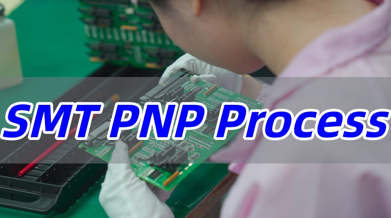
What Is SMT PNP Process?
The SMT PNP process—short for Surface Mount Technology Pick-and-Place process—refers to the automated operation where components are retrieved from feeders and accurately mounted onto a printed circuit board. This process is critical in modern electronics manufacturing because it directly impacts placement speed, accuracy, and final solder joint quality.
Key characteristics include:
- High-speed component mounting, often exceeding 30,000 components per hour.
- Vision-assisted alignment for components with fine pitches below 0.3mm.
- Support for a wide range of package types, from 01005 chip components to large QFPs and BGAs.
Without a well-tuned PNP process, downstream defects such as tombstoning, skewing, or poor soldering become inevitable.
What is the Difference between Pick and Place and SMT?
SMT refers to the entire surface mount technology process, which includes solder paste printing, component placement, reflow soldering, and inspection.
Pick and place is one specific step within the SMT process—the stage where components are actually placed onto the board.
Think of SMT as the overall assembly method and pick-and-place as the key action within that method.
Why SMT PNP Process Matters in Modern Electronics?
The SMT PNP process plays a vital role in modern electronics because it enables the assembly of miniaturized, high-density boards with high reliability and throughput. From smartphones to medical devices, precise component placement ensures signal integrity, thermal performance, and long-term functionality.
Key reasons for its importance:
- Miniaturization Support: Accurately places micro-components such as 0201 resistors and 0.35mm pitch BGAs.
- High-Speed Production: Modern multi-gantry PNP machines place tens of thousands of parts per hour, enabling mass production.
- Yield Improvement: Reduces misalignment and missing parts, which are common causes of post-reflow defects.
In applications like automotive control modules or wearable health monitors, a robust SMT pick and place process is non-negotiable for product durability and performance.
SMT PNP Process Step by Step
A well-defined SMT PNP process step by step ensures consistency and quality. Below is a simplified workflow:
- Board Loading and Alignment: The PCB is loaded onto the conveyor and clamped. Fiducial marks are scanned by the machine’s vision system to align the board coordinates.
- Component Picking: Nozzles pick components from tape-and-reel, tray, or stick feeders based on the programmed setup.
- Vision-Based Inspection: A camera checks the picked component for correctness, orientation, and lead coplanarity. Fine-pitch parts may require center-of-rotation correction.
- Placing: The component is placed onto the solder-paste-coated pad with a predefined pressure and precision—often within ±0.025mm.
- Post-Placement Inspection: AOI checks placement accuracy, presence, and polarity before the board proceeds to reflow soldering.
Following this structured SMT PNP process flow minimizes errors and ensures that all components are correctly positioned before the soldering stage.
What are the Different Types of Surface Mount Technology Machines?
A complete SMT production line consists of several key machines, each performing a specific role:
- Solder Paste Printer: Applies solder paste using a stencil.
- Solder Paste Inspector (SPI): Checks the volume, height, and alignment of the printed paste.
- Pick-and-Place Machine: The core of the SMT PNP process, places components automatically.
- Reflow Oven: Melts solder paste to form permanent electrical connections.
- Automated Optical Inspector (AOI): Examins the assembled board for defects.
Additional supporting equipment includes loaders/unloaders, glue dispensers, and rework stations.
Optimizing SMT PNP Process Flow for High-Quality Surface Mount Production
Optimizing the SMT PNP process flow involves fine-tuning both the equipment and the process parameters to maximize yield and minimize cycle time. Key strategies include:
- Line Balancing: Distributing placement tasks between multiple machines to avoid bottlenecks.
- Feeder Setup Optimization: Grouping components by usage frequency to reduce nozzle travel time.
- Preventive Maintenance: Regular calibration of nozzles, cameras, and feeders to sustain placement accuracy.
- Real-Time Monitoring: Using IoT-enabled sensors to track machine performance and preempt failures.
By implementing these measures, manufacturers can achieve a smooth, high-speed SMT PNP process flow capable of handling complex boards with high reliability.
How to Ensure the Advanced Surface Mount Pick and Place Accuracy?
High surface mount pick and place accuracy is achieved through a combination of machine capability, vision technology, and PCB design. Key factors include:
- Placement Accuracy: Defined as the deviation in X, Y, and θ (rotation). Modern placers achieve accuracy within ±25µm.
- Vision Alignment: Using upward and downward cameras to correct component position and rotation in real-time.
- Nozzle Selection: Different nozzle types are used to handle various component sizes and weights without dropping or damaging the part.
To quantify the impact of placement deviation on yield, the following formula can be applied:

Where Δx and Δy are offsets from the pad center, and σ is the standard deviation of placement accuracy.
Additionally, the maximum allowable rotation error θmax can be calculated as:
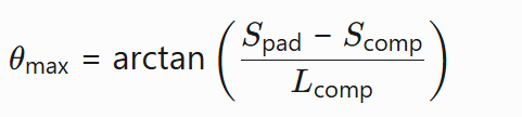
Where Spad is the pad size, Scomp is the component terminal size, and Lcomp is the component length.
By optimizing these parameters, manufacturers can ensure high reliability even with 01005 components or 0.3mm pitch BGAs.
EBest Circuit (Best Technology) – Technical Capability for Assembly Various PCB Types
At EBest Circuit (Best Technology), we specialize in SMT pick-and-place (PNP) assembly across a wide range of PCB types. From standard FR-4 to high-performance ceramic PCBs, our process ensures exceptional placement accuracy, reliability, and yield — no matter the complexity.
Our 3,000㎡ production facility is equipped for both prototype and mass production, supported by advanced process control and rigorous quality inspection.
1. FR-4 PCB Assembly
FR-4 boards remain the industry standard for consumer, telecom, and industrial electronics.
Our capabilities include:
- Multilayer boards up to 20 layers
- Accurate solder paste printing and reflow profiling
- Multiple surface finishes: ENIG, HASL, OSP
- Stable impedance control for signal integrity
We deliver consistent quality from small-batch prototypes to volume production, maintaining strong process repeatability.
2. Flexible PCB (FPC) Assembly
We provide advanced assembly for single-, double-, and multilayer flex PCBs made from polyimide (PI) or PET films.
Technical strengths:
- Fine line capability down to 0.04mm (1.5 mil)
- Laser-drilled micro-vias as small as 0.10mm for HDI designs
- Optional stiffeners (PI, FR4, or stainless steel) to enhance rigidity in selective areas
- Full turnkey service — from FPC design and material sourcing to SMT assembly and inspection
These assemblies are ideal for wearables, portable electronics, and other space-limited products.
3. Rigid-Flex PCB Assembly
Rigid-flex PCBs combine the mechanical strength of rigid sections with the flexibility of flex layers, reducing interconnects and improving durability.
Our process covers:
- Complex multilayer stack-ups
- Controlled impedance routing
- Reliable plated through-hole (PTH) interconnections
- Optimized lamination between rigid and flex areas
They are widely used in aerospace, medical, and industrial applications, where compact and rugged performance is essential.
4. Metal-Core PCB (MCPCB) Assembly
MCPCBs are designed for high-power and thermal-demanding environments.
Capabilities:
- Aluminum and copper cores with excellent heat dissipation
- Compatible with high-current LED and automotive lighting systems
- Controlled reflow process to avoid delamination and maintain flatness
Our process achieves reliable solder joints even under extended thermal cycling conditions.
5. Ceramic PCB Assembly
We assemble Al₂O₃ (alumina) and AlN (aluminum nitride) ceramic PCBs for RF, microwave, and aerospace electronics.
Highlights:
- Outstanding thermal conductivity and dielectric strength
- Precision handling to prevent substrate cracking
- Compatible with AgPd, Au, and ENEPIG surface finishes
These boards deliver exceptional stability in high-frequency and high-temperature environments.
Every assembly passes through a tightly controlled process chain:
- Incoming material inspection
- Automated solder paste printing & reflow profiling
- AOI, X-ray, and FCT testing
- Traceability through MES system
Our facility meets international quality standards: ISO 9001, ISO 13485, IATF 16949, and AS9100D, ensuring reliable results for every industry — from medical to aerospace.
In Summary, EBest Circuit (Best Technology) offers comprehensive assembly services for flex, rigid-flex, FR-4, metal-core, and ceramic PCBs, backed by precision equipment and strict quality control. We focus on high-yield, low-defect production, helping customers achieve consistent performance and long-term reliability in every design.
Why Choose EBest Circuit (Best Technology) for Reliable SMT PCBA Orders?
EBest Circuit (Best Technology) offers end-to-end SMT assembly solutions with an emphasis on precision, reliability, and traceability. Our advantages include:
1. High-Precision SMT Production Lines
Our SMT lines use advanced Yamaha and Siemens pick-and-place machines with intelligent vision alignment to guarantee precise placement — from 01005 chips to large BGAs.
We handle boards from 0.2×0.2 inches to 22×47.5 inches, supported by nitrogen-filled reflow ovens that minimize oxidation and deliver consistent solder joints with high first-pass yields.
2. Multi-Stage Quality Control
Quality is embedded in every step of our process, verified through multi-level inspection:
- 3D SPI: Checks solder paste volume, height, and alignment.
- 3D AOI: Verifies polarity, orientation, and solder joint integrity.
- X-Ray: Confirms hidden joints (BGA, QFN) without damage.
- FCT: Validates full functional performance before delivery.
Each inspection step ensures every board meets specifications the first time.
3. Certified Quality Management Systems
Our facility operates under internationally recognized standards:
- ISO 9001 for overall quality management
- ISO 13485 for medical electronics
- IATF 16949 for automotive-grade reliability
- RoHS & REACH compliance for environmental safety
These certifications reflect our long-term commitment to consistent quality and process discipline.
4. Full MES Traceability
Real-time tracking of each board through the entire SMT PNP process step by step.
- It records all process data — from paste printing to final inspection — giving you full traceability, process visibility, and data-driven quality assurance.
Any potential deviation is detected early, reducing downtime and ensuring on-time delivery. For more information or to send us an inquiry about rigid, rigid-flex, flex, IMS PCB, MCPCB, or ceramic base PCB, please email us at sales@bestpcbs.com.
In closing, we ensure that every board we build meets the highest standards of quality and reliability.
To conclude, the SMT PNP process is undeniably the backbone of high-quality surface mount assembly, impacting everything from production speed to long-term product reliability. By understanding its steps, optimizing its flow, and ensuring placement accuracy, manufacturers can achieve superior PCBA outcomes. At EBest Circuit (Best Technology), we combine state-of-the-art equipment with rigorous process controls to deliver SMT assembly services you can trust. For high-precision, high-yield PCBA solutions, please send us an email through the contact form at the bottom of our Contact US Page.