

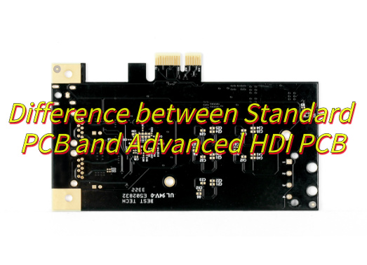
What is advanced HDI PCB? This blog covers structural differences, thermal performance, applications, and selection strategies between standard PCBs and advanced HDI PCBs.
Are you worried about these questions?
- BGA pitch at 0.4mm: yield stuck at 85%?
- Why 8-layer board costs 20% more than competitors?
- Design rework consumes 30% of R&D cycle?
As a HDI PCB manufacturer, EBest Circuit (Best Technology) can provide you service and solution:
- 30μm laser drilling: BGA yield at 0.35mm pitch improves to 93%
- Any-layer interconnect: 6-layer achieves 8-layer performance (IoT client cut costs by 18%)
- Free DFM report: blocks 80% of manufacturability issues upfront.
Feel free to contact us if you have any inquiry for HDI PCB fabrication: sales@bestpcbs.com.
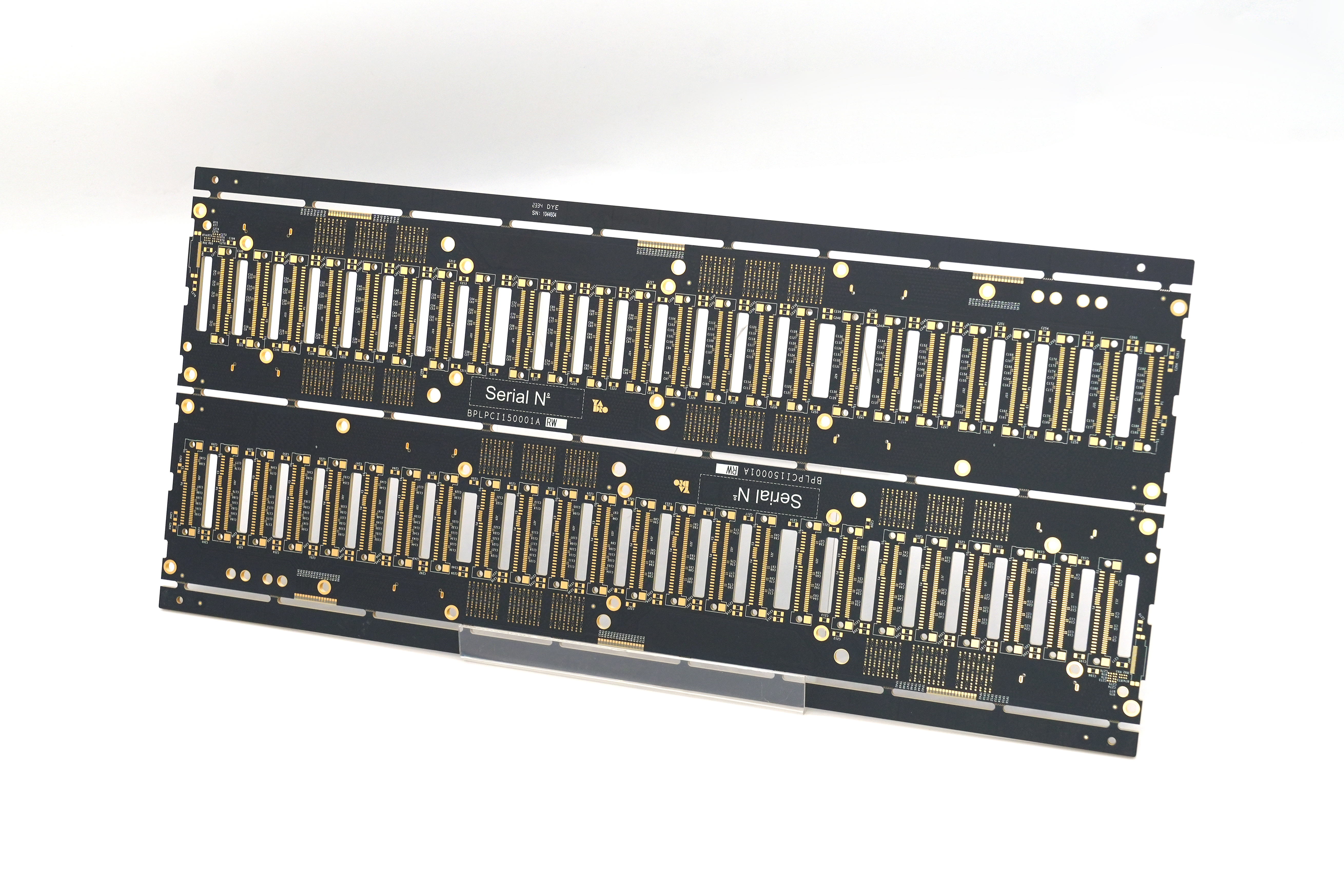
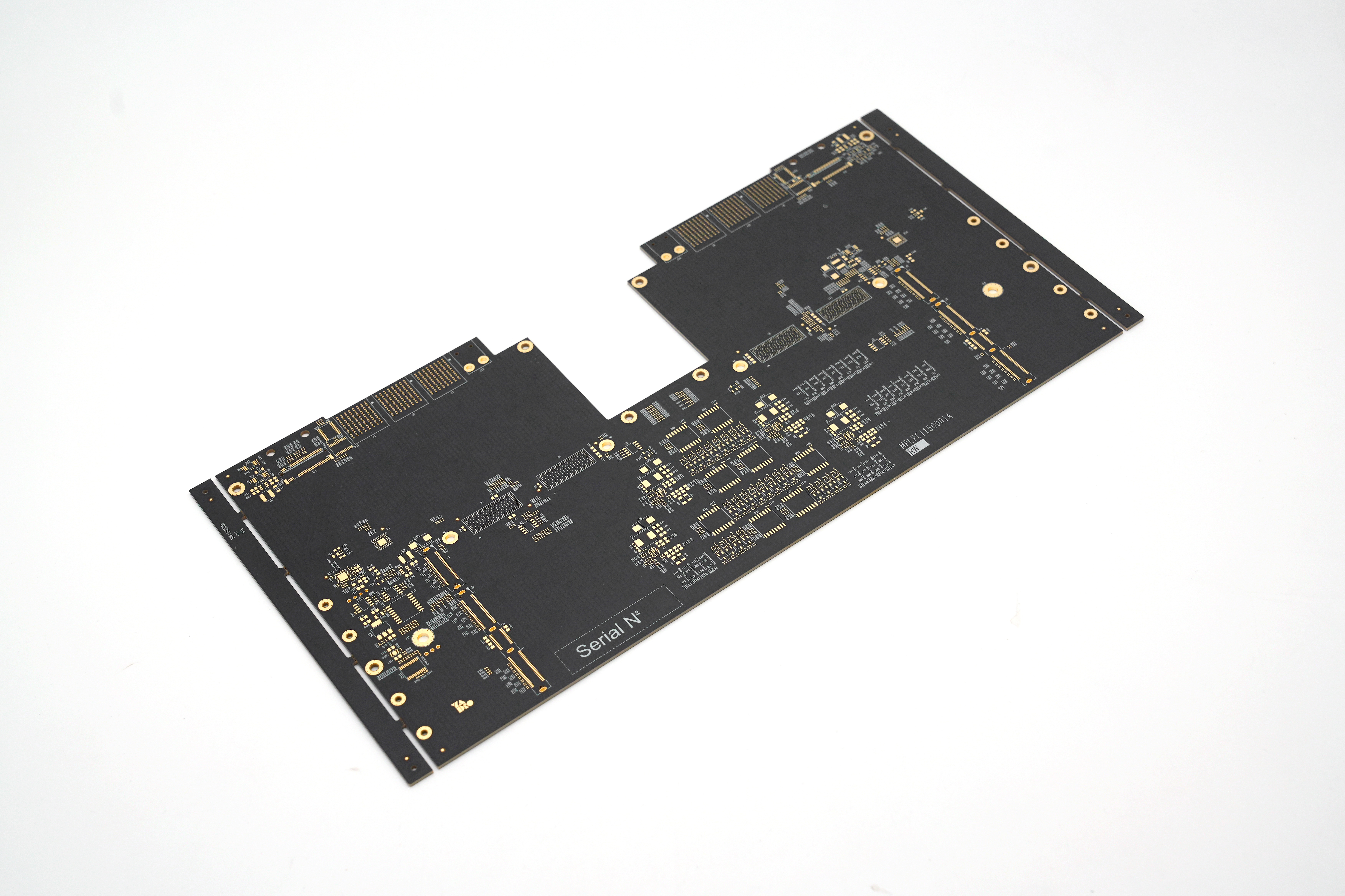
What Is Advanced HDI PCB?
Advanced HDI PCB (High-Density Interconnect Printed Circuit Board) is a multilayer circuit board technology characterized by ultra-fine wiring (under 100μm), microvias (blind/buried types), and high-density component placement. It achieves miniaturization through sequential lamination and laser-drilled microvias, enabling complex interconnections in compact spaces. This technology can supports high-speed signal transmission with controlled impedance and reduced parasitic effects.
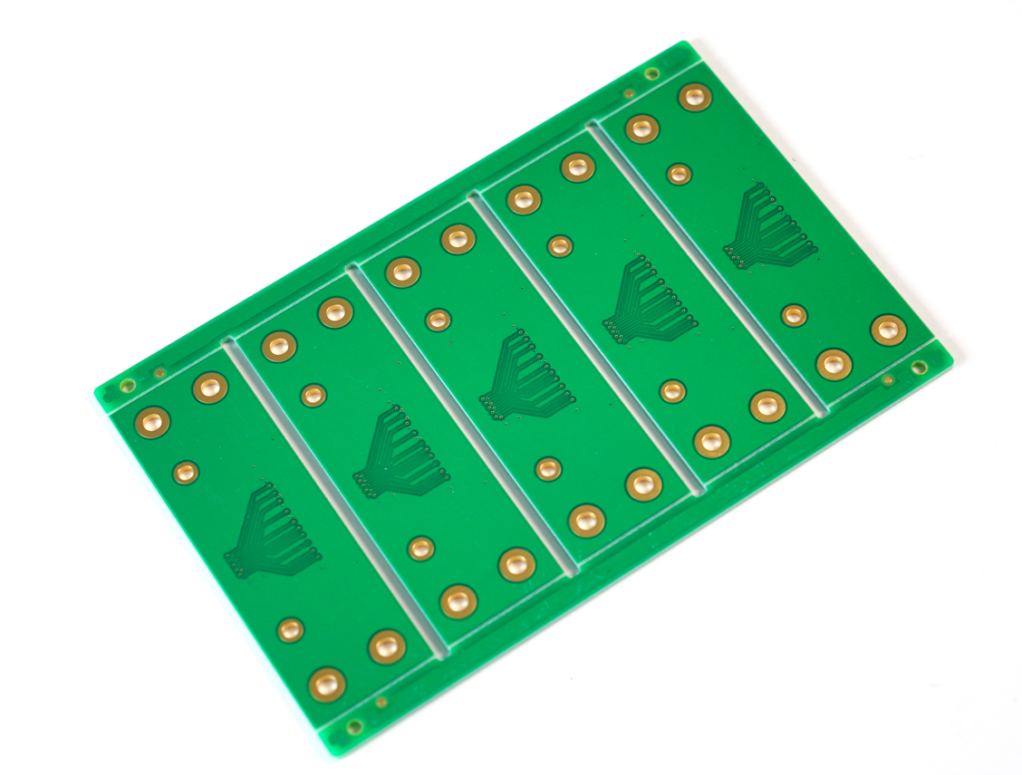
What Is Standard PCB?
Standard PCB refers to a conventional printed circuit board constructed with 1-16 conductive copper layers laminated with FR-4 epoxy substrate. Characterized by trace widths exceeding 0.15mm and through-hole interconnections, it accommodates components via surface-mount (SMT) or through-hole (THT) assembly methods. This cost-efficient design prioritizes manufacturability over high-density integration, serving as the baseline solution for mainstream electronics requiring reliable electrical connectivity without advanced miniaturization.
Difference Between Standard PCB and Advanced HDI PCB
1. Size and Weight
- Advanced HDI PCB: Typical thickness reduced to 0.4mm (e.g., smartphone motherboards), with weight reduction exceeding 30%. For example: Apple Watch S6 uses HDI technology, reducing motherboard area by 20% compared to previous models.
- Standard PCB: Conventional thickness ≥1.0mm, 10-layer board weight ≈ 120g/m² (e.g., power management boards in industrial control cabinets).
2. Component Density
- Advanced HDI PCB: Supports 20+ components/cm² (line width/spacing ≤40μm). For example, iPhone 17 Pro motherboard integrates over 1,000 components.
- Standard PCB: Density typically ≤5 components/cm² (line width/spacing ≥100μm), e.g., Arduino development boards accommodate only dozens of components.
3. Drilling Technology and Layer Count
- Advanced HDI PCB: Laser microvia diameter 50-100μm (mechanical drilling limit 200μm), with blind/buried vias accounting for >60%. Case: Huawei 5G base station RF module uses 8-layer HDI with 3-stage stacked vias, replacing traditional 16-layer designs.
- Standard PCB: Mechanical through-hole diameter ≥0.2mm, 6-layer through-hole boards cost 15% more than equivalent HDI boards (due to higher layer count requirements).
4. Manufacturing Cost
- HDI PCB: Unit price 30-50% higher, but system-level savings: Dell XPS laptops reduce PCB layers by 2 using HDI, cutting total costs by 12%.
- Standard PCB: 4-layer bulk price $0.5-2/sheet, but high-density needs require layer increases (each additional 2 layers raise costs by 35%).
5. Manufacturing Complexity
- HDI PCB: Requires 5+ lamination cycles (standard PCB: 1-2 cycles), with microvia copper filling defect rates <0.1% requiring nanoscale plating control.
- Standard PCB: Through-hole plating yield >98% (mature process),
6. High-Frequency and Thermal Management
- HDI PCB: Dielectric constant Dk ≤3.5 (high-frequency materials like Megtron 6), supporting 28GHz millimeter-wave. Case: Tesla autopilot modules reduce thermal resistance by 15℃/W using HDI embedded resistors.
- Standard PCB: FR-4 material Dk ≥4.5, with significant losses above 10GHz, relying on external metal layers for heat dissipation.
7. Reliability Data
- HDI PCB: Microvia thermal cycling test (-55℃~125℃) passes 3,000 cycles (JEDEC standard), but copper thickness inconsistencies cause 15% early failures.
- Standard PCB: Through-hole structures pass 1,500 thermal cycles, with typical failure mode being hole wall cracking (0.5% incidence).
Applications: Standard PCBs vs Advanced HDI PCBs
Standard PCB Applications
- Industrial Controls & Power Systems: Used in PLCs, motor drives, and power distribution units Automotive Electronics: Dashboards, engine control units (ECUs), and basic infotainment systems where space is less constrained.
- Consumer Appliances: Washing machines, refrigerators, and HVAC systems requiring simple circuit layouts.
- Low-Speed IoT Devices: Smart home sensors, basic monitors, and peripheral devices with minimal signal complexity.
Advanced HDI PCB Applications
- Mobile & Wearable Tech: Smartphones, smartwatches, and AR/VR devices demanding micro-sized components and high-speed connectivity.
- Medical Electronics: Implantable devices, portable ultrasound machines, and lab-on-a-chip systems requiring precision and miniaturization.
- 5G & Telecom Infrastructure: Base stations, mm Wave antennas, and data center interconnects for ultra-fast signal transmission.
- Aerospace & Defense: Avionics, radar systems, and satellite components needing lightweight, high-reliability circuits.
- AI & High-Performance Computing: Servers, GPUs, and neural processors requiring dense interconnects for efficient power delivery and thermal management.
Which Has Better Heat Dissipation: Standard PCB and Advanced HDI PCB?
Substrate Thermal Conductivity
- Standard PCB: Uses FR-4 substrate (0.3 W/m·K), relying on copper thickness (35–70μm) for heat dissipation.
- Advanced HDI PCB: Adopts high-thermal-conductivity resins/ceramic-filled substrates (1.0–2.0 W/m·K), though fine lines (<0.1mm) reduce copper cross-section.
Structural Heat Dissipation Efficiency
- Standard PCB: Thick copper layers enable horizontal heat spreading, suitable for <15W applications.
- Advanced HDI PCB: Microvia copper filling creates vertical thermal channels, reducing thermal resistance by 15–20% and cutting high-frequency temperature rise by 30% (ΔT 18°C vs. 22°C).
Thermal Accumulation Risk
- Standard PCB: Direct thermal paths in low-layer designs; multi-layer setups risk localized overheating.
- Advanced HDI PCB: 12+ layer stacks require rigorous thermal simulation, using embedded heat pipes/thermal via arrays to suppress interlayer thermal coupling.
Scenario Adaptability
- Standard PCB: Cost-effective, excels in <15W natural convection scenarios (7–10°C lower temp rise).
- Advanced HDI PCB: Optimizes high-density zones (e.g., 5G RF/GPU areas) via material + structural tweaks, limiting hotspot temp rise to <15°C.
Performance and Reliability: Standard PCB vs Advanced HDI PCB
Electrical Performance Differences
- Signal Integrity: Advanced HDI PCBs reduce signal path length by 30-50% through microvia/blind via technology, minimizing crosstalk and latency for 5G/high-frequency applications. Standard PCBs are better suited for low-frequency, simple circuits.
- Impedance Control: HDI’s laser-drilled microvias achieve ±3% precision (vs. ±10% for mechanical drilling in standard PCBs), ensuring stable high-frequency signal transmission.
Reliability Comparison
- Interlayer Connection: HDI’s Every Layer Interconnect (ELIC) technology reduces failure rates to 0.02% (vs. 0.1% for standard PCBs), doubling product lifespan.
- Thermal Stability: HDI uses high-Tg materials (≥180°C) and uniform copper thickness, reducing failure rates by 40% in high-temperature environments compared to standard PCBs.
Space & Cost Efficiency
- Miniaturization: HDI enables 60% higher component density for wearables/smartphones. Standard PCBs require larger board sizes (increasing costs by 15-20%).
- Long-Term Cost: HDI’s 30% higher upfront cost is offset by reduced layer counts (e.g., 8-layer HDI replacing 12-layer standard) and lower repair rates, achieving ROI within 2 years.
Production Flexibility
- Design Iteration: HDI supports 0.1mm line/space (vs. 0.15mm for standard), accelerating complex design iterations and cutting time-to-market by 1-2 months.
- Supply Chain Compatibility: Standard PCBs fit traditional equipment upgrades; HDI requires supplier capability assessment (only 12% of Chinese PCB factories excel in advanced HDI).
Environmental Compliance
- Material Standards: HDI commonly uses halogen-free substrates (IPC-4101E compliant), aiding EU RoHS 3.0 certification. Standard PCBs may require additional compliance costs.
How to Choose between Standard PCB and Advanced HDI PCB?
Design Complexity and Layer Count
- Standard PCB: Suitable for linear circuits with ≤10 layers and line width ≥100μm (e.g., industrial control boards). FR-4 substrate with traditional through-hole technology ensures short design cycles and controllable costs.
- HDI PCB: Ideal for high-density routing with ≥12 layers and line width ≤150μm (e.g., smartphone motherboards). Laser microvias and blind/buried via technology support high-pin-density BGA packaging.
Signal Performance
- High-frequency/high-speed scenarios (≥1GHz): HDI reduces parasitic capacitance/inductance by ~40%, enhancing signal integrity. Example: 28GHz mmWave module eye diagram margin improves from 0.3UI to 0.6UI.
- Low-frequency circuits (e.g., LED driver boards): Standard PCB’s through-hole technology meets requirements, with EMI issues optimized via ground layers.
Space & Component Density
- Space-constrained scenarios: HDI achieves 50μm line width/spacing, supporting BGA packages with >1500 pins, reducing area by 60% and thickness by 40%.
- Space-relaxed scenarios: Standard PCB’s 150μm line width/spacing lowers manufacturing difficulty and reserves space for heat sinks.
Cost & Lead Time
- Standard PCB: Unit cost ~$110-160/m², lead time 3-5 days. Bulk production (100k units) reduces total cost by ~40% compared to HDI.
- HDI PCB: Laser drilling and sequential lamination increase unit price, but reducing total layers (e.g., 8-layer HDI vs. 12-layer standard) cuts costs by ~15% while boosting signal speed by 50%. Lead time requires an additional 2-3 weeks.
Manufacturing & Design
- HDI Design: Adheres to “3-layer sequential lamination” limits; requires 3D simulation for via fill rate validation.
- Standard PCB Design: Supports relaxed DRC rules (line width tolerance ±20%), suitable for rapid prototyping.
Why Choose EBest Circuit (Best Technology) as Advanced HDI PCB Manufacturer?
Reasons why choose us as advanced HDI PCB manufacturer:
- 19 Years HDI Expertise: Specialized in high-complexity HDI manufacturing for 19 years, with 100,000+ batches delivered for 5G, medical, and automotive sectors, mastering microvia filling and layer alignment.
- 48-Hours Rapid Prototyping: Fast-track line ensures samples ship within 48 hours from design approval, speeding up validation for consumer electronics and automotive projects.
- Stringent Quality Certifications (ISO9001, ISO13485, and IATF16949): Ensures product consistency and compliance with global standards.
- Competitive Pricing: Affordable pricing without compromising quality, ideal for cost-sensitive projects.
- Six Layer Quality Inspection: Strict AOI, X-ray, and impedance testing reduce defects to <1%, meeting IPC-6012 Class 3 and ISO 9001:2015 standards.
- Free DFM Analysis: Complimentary design checks identify trace compliance, blind via feasibility, and thermal risks upfront to boost yields.
- Expert Technical Support: Senior engineers provide end-to-end guidance on HDI challenges like signal loss and thermal stress.
- Eco-Compliant Manufacturing: RoHS compliant processes and ISO certification support global environmental standards.
- Custom Application Solutions: Tailored designs address aerospace heat resistance, medical biocompatibility, and automotive vibration needs for precise performance.
Welcome to contact us if you have need any help for advanced HDI PCB board: sales@bestpcbs.com.
You may also like


Tags: Advanced HDI PCB, HDI PCB