Looking for copper metal core PCB thermal solution? Let’s explore spec, benefits, application, design guide and thermal solution, manufacturing process for copper metal core PCB.
Are you worried about these problems?
- Is your LED product experiencing luminous efficacy degradation due to insufficient heat dissipation?
- How can you avoid reliability risks when high-power devices experience uncontrolled temperature rise?
- Struggling to balance cost and performance? How can you choose a lightweight solution?
EBest Circuit (Best Technology) can provide solutions
- Precise Thermal Matching Service: Through thermal simulation modeling, we customize the copper layer thickness (available in 0.1-3.0mm), ensuring a 40% reduction in LED module junction temperature and a 50% reduction in lumen degradation.
- High-Current Wiring Technology: Utilizing an immersion gold (Immersion Gold) + OSP process, it supports a continuous current of 5A/mm², eliminating overheating issues in power modules and increasing yield to 99.2%.
- Lightweight Structural Design: Copper foil micro-etching technology achieves 50μm line/space widths. A multi-layer stacking solution reduces drone battery pack size by 20% and extends flight time by 15%.
Welcome to contact us if you have any request for metal core PCB: sales@bestpcbs.com.
What Is Copper Metal Core PCB?
A Copper Metal Core PCB (Printed Circuit Board) is a type of circuit board that uses copper as the base material instead of the traditional fiberglass (FR4). This metal core is typically located beneath the circuit layer and serves as a thermal conductor to dissipate heat generated by electronic components during operation. Copper metal core PCB has superior thermal conductivity, making it highly effective for managing heat in power electronics, LED lighting, automotive systems, and industrial control equipment.
Copper Metal Core PCB Specification
| Parameter | Specification |
| Base Material | Copper (typically C1100 or similar high-purity copper) |
| Copper Core Thickness | 0.5 mm, 1.0 mm, 1.5 mm, 2.0 mm, up to 5.0 mm (custom thickness available) |
| Circuit Layer Copper Thickness | 1 oz, 2 oz, 3 oz, up to 10 oz (35 µm to 350 µm) |
| Dielectric Layer Thickness | 0.05 mm to 0.5 mm |
| Thermal Conductivity of Dielectric | 1.0 W/m·K to 5.0 W/m·K or higher |
| Thermal Conductivity of Copper Core | ~400 W/m·K (excellent thermal performance) |
| Operating Temperature Range | -40°C to +150°C or higher depending on design |
| Surface Finish Options | HASL, ENIG (Electroless Nickel Immersion Gold), OSP, Immersion Tin/Silver |
| Solder Mask Color | Green, White, Black (custom colors available) |
| Board Size | Up to 600 mm × 1200 mm (larger sizes possible upon request) |
| Drilling Options | Mechanical drilling, laser drilling for micro vias |
| Layer Count | Single-sided, double-sided, multilayer (up to 4 layers typical) |
| Impedance Control | Available for RF/high-frequency applications |
| Certification Standards | ISO9001, UL, RoHS, IPC Class 2/3 compliant |
Benefits of Copper Substrate PCB
- Exceptional Heat Dissipation: Copper’s high thermal conductivity (2x aluminum) rapidly transfers heat away from components, preventing overheating in LEDs, power modules, or automotive systems.
- Longer Device Lifespan: Reduces thermal stress and component failure, extending reliability for high-current applications like EV chargers or industrial equipment.
- Compact Design Flexibility: Thick copper layers enable dense circuits and smaller boards, saving space in 5G devices, RF systems, or medical electronics.
- Cost-Effective Performance: Minimizes need for external cooling parts (fans/heatsinks), lowering long-term maintenance and material costs.
- Versatile Application Fit: Ideal for high-power (solar inverters), precision (aerospace), and EMI-sensitive (radar) designs, ensuring stable operation in extreme environments.
Applications of Copper Metal Core PCBs
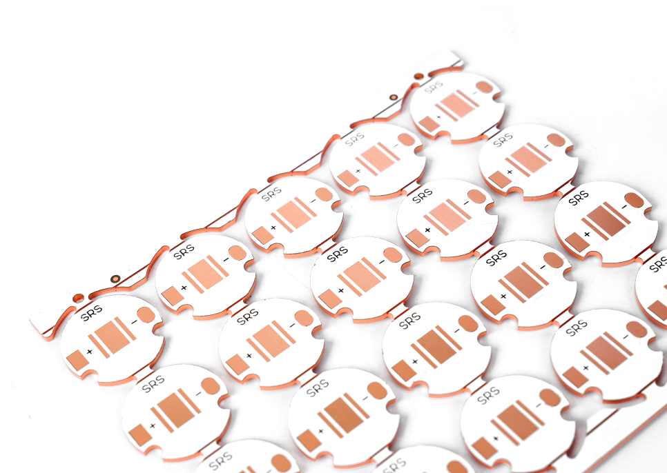
- High-Power LED Lighting: Efficiently dissipates heat from dense LED arrays, preventing color shift and extending lifespan for automotive, industrial, and architectural lighting.
- Automotive Electronics: Manages heat in power modules (e.g., engine control units, battery management systems) under extreme temperatures, enhancing reliability for EVs and hybrid vehicles.
- 5G & RF Devices: Supports high-frequency circuits and millimeter-wave components by minimizing thermal noise, critical for 5G base stations and radar systems.
- Industrial Power Systems: Withstands high currents and thermal stress in motor drives, inverters, and solar power converters, reducing downtime and maintenance costs.
- Aerospace & Defense: Provides lightweight, durable thermal management for avionics, satellite components, and ruggedized communication gear in harsh environments.
Copper Metal Core PCB Design Guide
Below is copper metal core PCB design guide:
1. Material & Substrate Selection
- Use copper-core substrates (thermal conductivity ≥2W/mK) or ceramic substrates (AlN, 320W/mK). Avoid FR4.
- High-power areas: 3-4oz copper; peripheral zones: 2oz. Transition zones use teardrop shapes (≤45°).
- Ensure lead-free solder (SAC alloy), halogen-free laminate, and RoHS/REACH compliance.
2. Thermal Management
- Spread high-power components (e.g., power ICs) to prevent heat buildup. Place heat-generating parts on outer layers for direct cooling.
- Thermal vias: 0.3mm diameter, ≥4 vias/cm², 30μm copper plating. For IGBTs, embed 1.5mm heat pipes (local temp rise ≤15°C).
- Add 10μm graphene film on copper layers to boost thermal diffusion by 40%. Validate designs with ANSYS/Flotherm and IR thermography.
3. Stack-Up & Board Thickness
- For RF circuits, use Rogers RO4000 (Dk=3.38). Multi-layer boards: 6 layers reduce crosstalk by 60-70% vs. 4 layers. Apply 20H rule (power plane indented 20× layer spacing).
- Standard thickness: 1.6mm; use ≥2.0mm for high-power applications.
- Maintain >85% copper uniformity. Blind/buried vias reduce thermal stress by 30%.
4. Routing & Signal Integrity
- Track width: 1mm (1oz copper) = 1A. Widen tracks for high current (1A/0.3mm). Prioritize power traces to minimize impedance.
- High-speed signals: 3W spacing, matched lengths, 135° bends. Crystal circuits: Ground enclosure with stitching vias.
- Route critical signals (e.g., clocks) first. Bridge splits with 0.1μF + 10μF capacitors.
5. Vias & Solder Mask
- Laser vias: ≥0.1mm; mechanical vias: ≥0.2mm. Tolerance ±0.05mm (≤0.8mm vias). High-speed vias: Stub length <10mil; back-drill tolerance ±2mil.
- Solder mask: Expand 0.05-0.1mm beyond pads. For BGAs, use NSMD (mask opening 15-25μm larger than pad). Remove mask in thermal zones.
6. Manufacturing & Testing
- Hole aspect ratio (diameter:total thickness) ≤10:1. Metal-base tolerance: ±0.1mm; add 0.3mm vent holes per 20×20mm.
- Reliability tests: Environmental: Thermal cycle (-40°C/+125°C), 95%RH/40°C/96h. Mechanical: Tensile strength >10N; peel strength ≥1.0N/mm.
- Electrical: Contact resistance (mΩ-Ω range); insulation >10⁷Ω; HiPot.
7. Special Applications
- High-power modules: Step-down copper (4oz core, 2oz periphery); embed AlN or heat pipes.
- Flex designs: Rigid-flex follows rigid rules; keep 1.5-2mm clearance from SMD outlines.
- Low-temperature: Use high-Tg substrate (Tg>170°C); increase via density.
Copper Metal Core PCB Thermal Solution
1. Advanced Thermal Materials
- Graphene-Enhanced Copper: Utilize copper-graphene composites (thermal conductivity up to 440W/mK) for core heating zones. Apply 10μm graphene films on copper layers to boost lateral thermal diffusion by 40%.
- Staged Copper Thickness: Use 4oz copper for high-power areas (e.g., IGBTs), transitioning to 2oz in peripheral zones via teardrop-shaped (≤45°) connections.
2. Via Array Optimization
- Thermal Vias: Deploy 0.3mm diameter vias in hotspots (density ≥4 vias/cm²), reducing thermal resistance by 90% compared to non-via designs.
- Dynamic Spacing: Use hexagonal via patterns for heat flux >50W/cm²; rectangular arrays for <30W/cm². Maintain via spacing ≥2×via diameter +0.1mm.
- Copper-Via Synergy: Thicken via walls to ≥30μm when outer-layer copper exceeds 35μm. Reduce via spacing to 0.8mm for 35μm copper layers.
3. Heat Pipe Integration
- Embedded Heat Pipes: Insert 1.5mm-diameter heat pipes beneath IGBTs, filled with phase-change material. Limits local temperature rise to ≤15°C (5× more efficient than vias alone).
- Patent-Proven Designs: Fix heat pipes to aluminum substrates via high-temperature soldering, ensuring direct contact with chassis for efficient heat dissipation.
4. Thermal Path Engineering
- Vertical-Horizontal Hybrid Cooling: Combine 0.3mm vias (vertical heat transfer) with 0.5mm linewidth hexagonal grids (horizontal spreading) in non-critical zones.
- Ceramic Insertion: Embed AlN ceramic pads (thermal conductivity 320W/mK) under power modules, bonded with silver paste to achieve baseplate thermal resistance <0.15°C/W.
5. Simulation & Validation
- Thermal Modeling: Use ANSYS Icepak with 3× denser mesh in via regions. Validate against real-world data (e.g., 48V DC/DC module via optimization reduced thermal resistance from 1.2°C/W to 0.78°C/W).
- Infrared Testing: Confirm design efficacy via thermal imaging, ensuring peak junction temperatures stay below 125°C (with <10°C rise per 10% power increase).
6. Manufacturing Adjustments
- Aspect Ratio Control: Maintain via diameter-to-board thickness ratio ≤10:1. Tolerance: ±0.05mm for vias ≤0.8mm.
- Solder Mask Management: Expand solder mask 0.1mm beyond pads; remove mask entirely in thermal via arrays to enhance heat dissipation.
How to Make A Copper Metal Core PCB?
1. Material Preparation
- Substrate Selection: Choose copper-core substrates (thermal conductivity ≥2W/mK) or ceramic substrates (AlN, 320W/mK). Avoid FR4.
- Copper Foil: Use 3-4oz copper for high-power areas; 2oz for signal layers. Pre-treat copper surfaces for adhesion.
- Auxiliary Materials: Prepare dry film, solder mask ink, and semi-cured sheets (PP) for lamination.
2. Inner Layer Fabrication
- Surface Cleaning: Clean substrates to remove oils, oxides, and contaminants.
- Dry Film Application: Lamination of photosensitive dry film on copper surfaces.
- Exposure & Development: UV exposure transfers circuit patterns to the dry film. Unexposed areas are dissolved in developer solutions.
- Etching: Remove unprotected copper using alkaline etchants (e.g., ammonium persulfate).
- AOI Inspection: Automatic Optical Inspection (AOI) detects defects like opens/shorts.
3. Lamination
- Stack-Up: Align inner layers, PP sheets, and outer copper foils per design. Use pins/optical alignment for precision.
- Pressing: Apply heat (180–220°C) and pressure (1.5–2.5MPa) to melt PP and bond layers. Maintain vacuum to eliminate air bubbles.
- Post-Press Treatment: Cool boards gradually to avoid warping. Trim edges and remove excess PP.
4. Drilling & Plating
- Mechanical/Laser Drilling: Drill through-holes, blind/buried vias. Laser drilling is used for microvias (<0.15mm).
- Deburring: Remove drill swarf and smooth hole walls.
- PTH (Plated Through-Hole):
- Desmearing: Clean hole walls with plasma/permanganate.
- Chemical Deposition: Coat holes with a thin copper layer (1–2μm).
- Electroplating: Thicken copper to 20–40μm for conductivity and durability.
5. Outer Layer Fabrication
- Dry Film Application: Repeat processes for outer layers.
- Exposure/Development/Etching: Similar to inner layers but with tighter tolerances.
- Tin Plating (Optional): Electroplate tin as an etch resist for selective copper retention.
6. Solder Mask & Silkscreen
- Solder Mask Application: Coat boards with liquid photoimageable solder mask (LPI).
- Exposure/Development: Expose mask to UV light, leaving pad areas uncovered.
- Curing: Bake boards to harden the mask.
- Silkscreen Printing: Add component labels, logos, and markings using UV-curable ink.
7. Surface Finish
- HASL (Hot Air Solder Leveling): Dip boards in molten solder, then level with hot air. Cost-effective for general use.
- ENIG (Electroless Nickel/Immersion Gold): Deposit nickel (3–5μm) and gold (0.05–0.1μm) for flat surfaces and corrosion resistance.
- OSP (Organic Solderability Preservative): Apply a thin organic layer for lead-free compatibility.
8. Routing & Testing
- CNC Routing: Cut boards to final dimensions using milling machines. Add V-scores for easy breaking.
- Electrical Testing:
- Flying Probe: Check for opens/shorts with movable probes.
- Fixture Test: Use bed-of-nails for high-volume inspection.
- Final Inspection: Visual check for defects (e.g., solder mask bridges, misalignment).
9. Packaging & Shipping
- Vacuum Packing: Seal boards in anti-static bags with desiccants.
- Labeling: Include PCB specs, date codes, and compliance marks (RoHS, UL).
Why Choose EBest Circuit (Best Technology) as Metal Core PCB Manufacturer?
- Global ISO/RoHS/REACH/UL Compliance: One-step certification for EU/US markets.
- Free DFM Support: Avoid costly redesigns with first-pass success guarantee.
- 1 Piece MOQ & 24-Hour Rapid Prototyping: Accelerate product validation by 5x, beat competitors to market.
- A Week Mass Production Turnaround: Eliminate supply chain bottlenecks during peak seasons.
- Thermal Performance Optimization: Reduce power module temperatures by 25%, extend product lifespan.
- Strict Quality Inspection: Conduct full inspection in batches and strictly control quality to reduce the cost of rework for customers.
- Competitive Price: Transparent Price Structure, No hidden Cost to be incurred.
- Cost-Efficient Material Solutions: Achieve 15% higher profitability for LED/5G products.
- High-Density Routing Expertise: Miniaturize IoT devices without sacrificing performance.
Welcome to contact us if you have any request for metal core PCB: sales@bestpcbs.com. Looking forward to hearing from you soon!