





Closer thermal via spacing helps only if the via barrels are a meaningful part of the heat path. Before packing more vias under a QFN pad, compare the two arrays on the same copper and stackup, check that the solder joint still forms correctly, and repeat the temperature test at the same power and airflow.
Thermal Via Spacing
Thermal via spacing is the center-to-center distance between vias that transfer heat through the board. It does not determine temperature on its own. The pad size, via diameter and plating, copper planes, and the path from the board to air or a heatsink all matter.
Consider a hypothetical power QFN with a 3 × 3 via array. The board runs hotter than expected at a steady load. The designer wants to change only the via count. Compare that option with improving copper spreading or the board-to-heatsink interface before assuming pitch is the limiting variable.
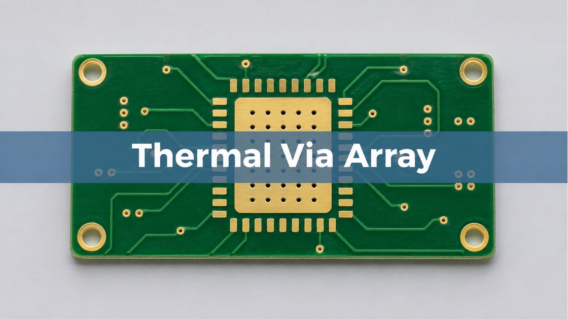
Thermal Via Array
Compare arrays that fit in the same usable pad region. In this example, a 3 × 3 array at 1.00 mm pitch and a 4 × 4 array at about 0.667 mm pitch each span 2.00 mm between outer via centers. Neither value includes the via land radii, required edge margin or paste pattern.
| Parameter | Array A | Array B |
| Via count | 9 | 16 |
| Center pitch | 1.00 mm | About 0.667 mm |
| Outer-center span | 2.00 mm | 2.00 mm |
| Via barrel and stack | Same assumed geometry | Same assumed geometry |
Overlay the copper, drill and stencil data. An array that fits by center points alone may not leave enough room for the actual lands, mask or paste windows.
Thermal Via Diameter
Distinguish the finished hole diameter from the drilled hole and pad diameter. For a simplified barrel with 0.25 mm inner diameter and 0.025 mm wall thickness, the outer barrel diameter is 0.30 mm. The land can be wider. A larger land does not add the same axial copper area as a thicker barrel.
Ask for the approved drill, plating and via construction. Via fill and surface finish also affect the assembly decision. Use the package supplier’s land and stencil guidance for the actual component instead of borrowing a via diameter from a different exposed pad.
Thermal Resistance of PCB Vias
The barrel conducts heat along its copper wall. The cross-sectional area is π ÷ 4 × (outer diameter² − inner diameter²). In the illustrative geometry it is about 0.0216 mm². Do not count the air in an open hole as solid copper.
Assume uniform copper, equal temperature at all top via ends and equal temperature at all bottom ends. This idealization lets the barrel conductances add in parallel. It does not account for how heat spreads across the pad or through the receiving plane.
Thermal Resistance Formula Conduction
For one uniform conduction path, thermal resistance is length divided by conductivity times cross-sectional area: R = L ÷ (k × A). At 1.60 mm length, an illustrative copper conductivity of 390 W/(m·K), and 0.0216 mm² of wall area, one barrel is about 190 K/W. Convert mm and mm² to meters and square meters first.
Under the equal-end-temperature assumption, nine barrels give about 21.1 K/W and sixteen give about 11.9 K/W. This is a barrel-only estimate, not a junction-to-ambient rating. If both arrays connect into a poorly spreading region, the assembled temperature difference may be much smaller.
Thermal Via Solder Wicking
Check the solderable pad before approving a denser pattern. Open holes can draw solder away from the joint. More vias can change available paste area and the joint’s void pattern. Review the package recommendation, assembly process and available via treatments together.
See the Best Technology guide to solder wicking through thermal vias for the joint-side checks. Use the agreed inspection method and joint acceptance criteria; a lower board temperature does not excuse a failed solder joint.
PCB Thermal Resistance
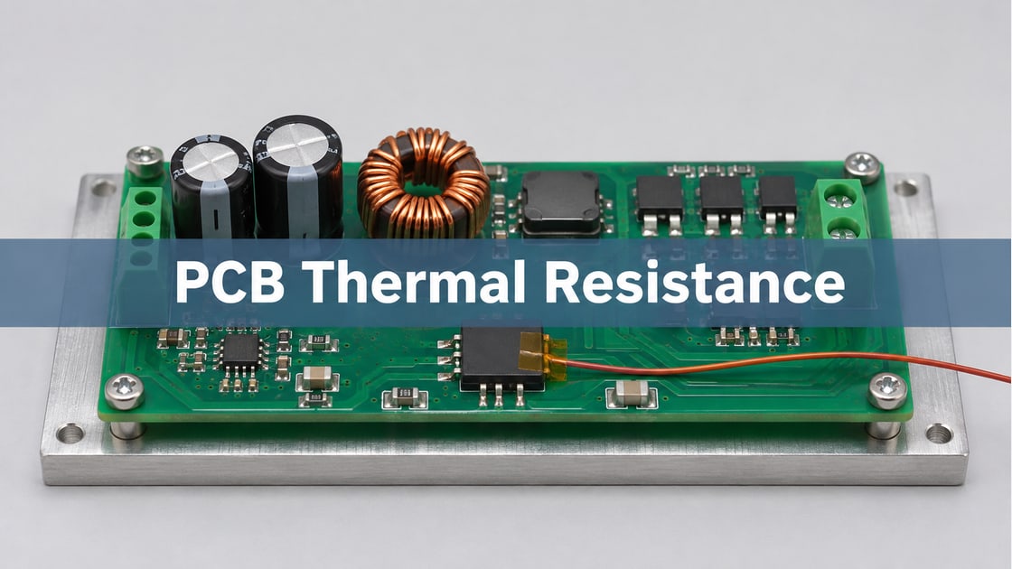
Interpret the temperature result as a system measurement. Hold the copper layout outside the test pad, component, board stackup, heatsink contact, airflow, ambient and actual dissipated power as constant as practical. Measure at the same defined point and after a comparable steady-state condition.
| Observation | Decision |
| Denser array lowers temperature repeatably | Verify joint quality and final conditions |
| Both arrays run similarly | Investigate spreading, interface and airflow |
| Denser array harms the joint | Change via treatment or paste plan before release |
| Power or airflow changed | Repeat the controlled comparison |
If the product limit is junction temperature, use an appropriate package method for estimating or measuring it. A board thermocouple at an arbitrary spot is not a direct junction measurement.
Thermal Via Design Guidelines
Approve the densest pattern only if it earns its manufacturing cost and passes the real requirements. Check DFM, repeat temperature measurements at the agreed operating conditions, and verify the assembly evidence. If the gain is within measurement scatter, investigate a different bottleneck rather than declaring the denser pitch a fix.
Record via count, construction, dimensions and the validated setup. If the copper stack, heatsink interface or stencil changes later, revisit the result rather than assuming the same spacing still works.
Frequently Asked Questions
Is there one recommended spacing for thermal vias?
No universal pitch fits every package or process. Use the exact component’s land-pattern guidance, the fabricator’s approved drill and copper rules, and the assembler’s paste requirements. Check the outer via margins and then compare temperature on representative hardware before approving a denser array.
Why is the calculated resistance of one via so high?
A plated barrel has a thin conducting wall. Even though copper conducts heat well, the wall area is small relative to the length of a through-board path. Several barrels can reduce that segment’s resistance in parallel, but they do not remove the other limits in the system.
Can I use the pad diameter to calculate barrel area?
No. The pad diameter describes the copper land at a layer, not the cross section of the barrel conducting through the board. Use the wall geometry and the appropriate conductive length for that model. Model any approved conductive fill separately rather than counting the whole pad as axial copper.
Can a solid fill always be treated as copper?
No. Fill materials can have different conductivities, and some fill is used for planarization rather than as a high-conductivity path. Ask for the qualified material and construction. Use its relevant properties in the model, and keep the solderable surface requirement separate from the thermal calculation.
Should every thermal via connect to a ground plane?
Only if the package electrical requirements and board design allow that connection. The exposed pad may have a specified potential. Verify the datasheet and intended planes before adding vias. A good heat path is not acceptable if it shorts nodes or violates the component’s electrical layout rules.
What if a denser array changes the temperature only slightly?
Repeat at the same power and ambient with the same sensor placement. If the change is within normal measurement scatter, do not credit the array. Check the receiving copper, thermal interface and airflow before spending more on via count, fill or additional fabrication operations.
Can I compare an infrared reading with a thermocouple reading?
Only after accounting for what and where each instrument measures. Infrared readings depend on emissivity and spot size; a contact sensor depends on placement and attachment. Define a repeatable point and method for the comparison. Do not combine unrelated readings as if they measured the same temperature.
What should be included in a thermal via fabrication review?
Send the package land pattern, stackup, drill and finished-hole data, plating requirements, pad and stencil layout, and the planned temperature test. Identify the operating power and limit you must meet. That gives the reviewer enough context to compare array geometry with fabrication and assembly constraints.
References
Discuss Your PCB Requirements
For a Best Technology fabrication review, send the component pad drawing, candidate arrays and layer stack to sales@bestpcbs.com. Include the proposed via treatment and the temperature test conditions so the drawing review addresses the actual build.
You may also like



Tags: PCB Temperature Testing, QFN Via Array, Thermal Via Spacing, Via Barrel Resistance