Sensor PCB manufacturing brings together the circuit board, sensing components and assembly processes that a measurement device needs to operate reliably. From temperature monitoring and pressure measurement to motion detection and connected equipment, the board must support the sensor electrically while preserving its mechanical, thermal and environmental requirements.
At EBest Circuit, we provide custom PCB fabrication, component sourcing and SMT/THT assembly for sensor electronics. Our work includes coordinating board specifications with assembly requirements, inspecting solder joints and arranging functional testing to the agreed product specification. Discuss your sensor board prototype or production build with us at sales@bestpcbs.com.
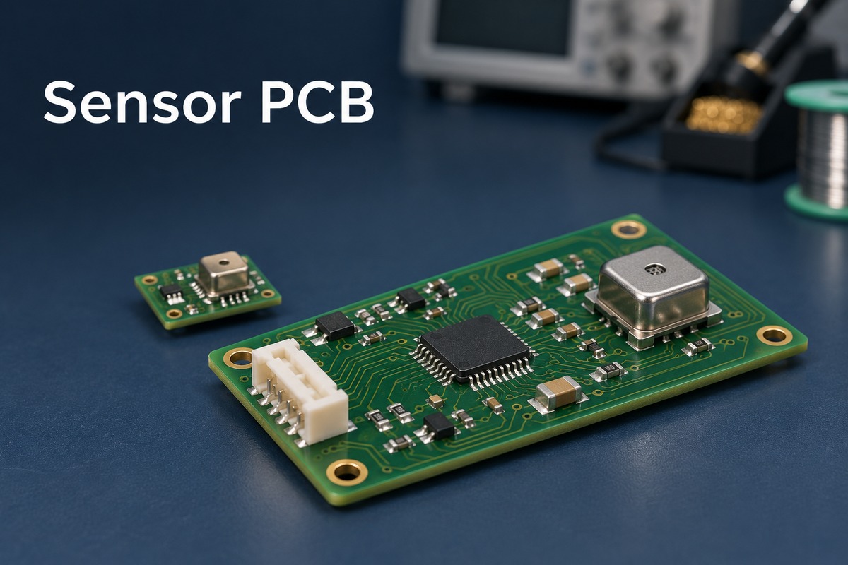
PCB Sensor Board Types and Applications
A PCB sensor board carries a sensing device, connects to an external transducer, or combines several sensing channels with a controller. Each type places different demands on the board and assembly process.
| Board type | Typical use | Key process focus |
|---|---|---|
| Temperature | Thermal monitoring | Thermal paths |
| Humidity | HVAC monitoring | Sensing-area protection |
| Pressure | Instrumentation | Port clearance |
| Motion | Movement detection | Orientation and stress |
| Optical | Object detection | Alignment and cleanliness |
| Current | Power monitoring | Current path and isolation |
These differences affect the physical build. An ambient temperature sensor may need isolation from a warm regulator; a sensor measuring a nearby component needs thermal coupling to that component. In optical sensor PCB assembly, the sensing face must align with the intended optical path.
We supply both bare boards and assembled sensor boards. Bare boards provide the interconnections; assembled boards add the specified sensors, supporting components and connectors.
Custom Sensor PCB Board Manufacturing Capabilities
EBest Circuit manufactures custom sensor PCBs with multilayer stackups, fine routing and controlled mechanical dimensions. Our capabilities support compact sensor interfaces, supporting electronics and board mounting requirements.
| Manufacturing feature | Standard capability | Special-process capability |
|---|---|---|
| FR4 layer count | 1–10 layers | Up to 32 layers |
| Trace/space, 1 oz inner/outer copper | 4/4 mil | 3/3 mil |
| Minimum finished hole | 0.20 mm | 0.15 mm |
| NPTH diameter tolerance | ±2 mil | ±1 mil |
| PTH diameter tolerance | ±3 mil | ±2 mil |
| Green solder-mask bridge, 1 oz copper | 4 mil | 3 mil |
Material options include standard, mid-Tg and high-Tg FR4, including IT180 and Shengyi S1000-2. Additional capabilities include 0.10 mm laser-drilled blind vias, ±5 mil standard outline tolerance and ±1 mil solder-mask registration.
Surface finishes include ENIG, OSP, HASL, immersion silver, immersion tin and ENEPIG. For ENIG, the available thickness range is 0.025–0.125 µm gold over 3–8 µm nickel.
Our DFM review checks routing, holes and solder-mask features against the selected stackup and copper weight. Special-process limits are assessed for the complete design rather than assumed to be available in every combination.
Precision Sensor PCB Assembly Service
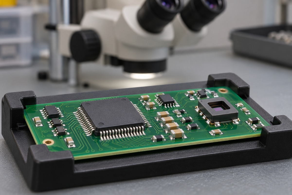
Our precision sensor PCB assembly service combines SMT, through-hole or mixed assembly with handling suited to the selected sensing device. The process must preserve sensing openings and package integrity as well as form reliable solder joints.
- Paste and placement. Apertures, paste volume and component seating must suit the footprint. For compact controllers and supporting ICs, fine pitch PCB assembly also requires inspection appropriate to the joint geometry.
- Reflow control. The profile must respect the exact component’s thermal limits, including any subsequent soldering or repair operation.
- Cleaning and coating. Follow the sensor’s material restrictions and protect exposed sensing elements. A process suitable for other board components may damage the sensor.
- Handling and depaneling. Support the board during separation, connector insertion and mounting to limit stress transferred to sensitive packages.
For example, Sensirion SHTxx humidity and temperature sensors prohibit board washing and exposure to cleaning agents, and require sensing-element protection during coating. These restrictions apply to that device family, not every sensor board.
Assembly inspection verifies workmanship. Measurement accuracy additionally depends on the circuit, calibration and final installation, so a precision measurement requirement needs a defined performance test.
Turnkey IoT Sensor PCB Assembly and Component Sourcing
Turnkey IoT sensor PCB assembly coordinates board fabrication, parts procurement and assembly. EBest Circuit supports full turnkey PCB assembly, partial turnkey and consigned builds.
| Supply model | Who supplies parts? | Best fit |
|---|---|---|
| Full turnkey | EBest Circuit | One coordinated order |
| Partial turnkey | Customer + EBest | Selected customer-held parts |
| Consigned | Customer | Existing component inventory |
We source components from manufacturers or authorized distributors. Three details are especially important for sensor BOMs.
- Exact ordering code. Parts in one family can differ in measurement range, accuracy grade, interface and package.
- Approved alternatives. A matching footprint does not establish equivalent sensing behavior or firmware compatibility.
- Build revision. The hardware, firmware and test requirements must describe the same product configuration.
A long-lead sensor or wireless module can determine the build schedule even when all other components are available. Turnkey assembly covers the agreed manufacturing scope; software development and measurement algorithms require separate arrangements.
Quality Control and Testing for Sensor PCB Assemblies
Sensor PCB quality control covers manufacturing defects and the specified behavior of the powered board. EBest Circuit uses SPI, AOI and X-ray inspection, with functional testing arranged around the project requirements.
- Solder-paste inspection. SPI checks deposition before component placement.
- Assembly inspection. AOI examines visible features; X-ray helps inspect hidden joints.
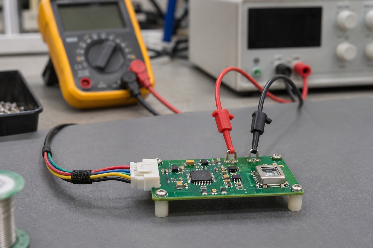
- Functional testing. Defined tests can check communication, supply current and response to a controlled input.
- Calibration, when specified. Suitable reference equipment and a defined procedure establish or adjust the relationship between input and reported output.
A changing sensor reading is not proof of measurement accuracy. A useful functional test specifies both the stimulus and acceptance limits. Calibration is a separate operation and is not implied by AOI, X-ray or a general functional-test step.
Final-product validation may also need the enclosure. Airflow, optical windows and mechanical mounting can change sensor behavior after an otherwise acceptable board leaves assembly.
PCB Sensor Board Prototyping and Production Lead Times
Sensor PCB lead time combines fabrication, procurement, assembly and testing. Some activities can run in parallel, but assembly needs both usable boards and the required components.
Our normal standard FR4 prototype fabrication references are below, for qualifying builds under one square meter.
| Layers | Fabrication reference |
|---|---|
| 1 | 7 days |
| 2 | 8 days |
| 4–6 | 10 days |
| 8 | 12 days |
These references apply to standard prototype specifications, including 0.4–1.6 mm FR4, standard copper options, lead-free HASL and conventional geometry. The quotation confirms the applicable schedule and current availability.
- Custom fabrication. ENIG, special materials or tighter features can change the board schedule.
- Component procurement. A sensor or module shortage can hold up an otherwise ready build.
- Assembly and testing. Fixture preparation and agreed test operations add time beyond bare-board fabrication.
- Repeat production. Released data and an established BOM reduce preparation, while batch quantity and production loading still affect scheduling.
The table is a bare-board reference, not a complete PCBA delivery promise. Shipping time is additional.
Custom Sensor PCB Manufacturing Case Study
An EBest Circuit project for a US customer involved matching top and bottom sensor-board variants. The order specified four-layer FR4 fabrication, full component sourcing and SMT assembly, with 50 units plus one spare for each variant.
| Parameter | Project specification |
|---|---|
| Construction | 4-layer FR4, IT180A |
| Board thickness | 1.006 mm ±10% |
| Inner / outer copper | 1 oz / 1 oz |
| Finish | ENIG, Au 2 µin |
| Mask / legend | Red / white |
| Through-hole / via tolerance | ±77 µm |
| Hole copper | 38 µm ±12 µm |
Three requirements shaped the production plan.
- Drilled locating holes. Four designated holes on the top-board outline provided positioning and required drilling rather than CNC outline routing. Other edge features without a locating function could be routed.
- Panel-to-unit handoff. Fabrication required panel delivery, while SMT instructions called for individual assembled boards. The production sequence had to accommodate both forms.
- Cleanliness and packing. Assembly instructions required board surfaces free of foreign matter and antistatic-bag packaging.
This project illustrates how mechanical features, board specifications and assembly requirements connect. The parameters above apply to these two variants, rather than every sensor PCB.
Why Choose EBest Circuit for Sensor PCB Manufacturing?
EBest Circuit brings PCB fabrication, component sourcing and assembly into the same project discussion. That coordination matters when a sensor board has requirements that cross process boundaries, such as locating features, protected sensing areas or a specific delivery form after assembly.
- Fabrication linked to assembly. Board construction, surface finish and panel arrangements can be considered alongside the component packages and final assembled format.
- Flexible sourcing arrangements. Full turnkey, partial turnkey and consigned supply allow the purchasing model to match the customer’s control of sensors and other critical parts.
- Inspection matched to the build. SPI, AOI, X-ray and project-defined functional tests address different defect and performance questions instead of treating one inspection method as a complete quality assessment.
- Experience with detailed sensor-board requirements. The top-and-bottom board project illustrates attention to positioning features, specified laminate and component sourcing within one manufacturing scope.
For a sensor product, a useful manufacturing partner understands how these requirements connect. Our quotation can bring the board, BOM, assembly scope and agreed test needs into one build plan.
FAQs About Sensor PCB Manufacturing and Assembly
Can the sensor be mounted away from the main PCB?
Yes. A separate sensor board or cable-connected sensing element can place the measurement point closer to the target. The interconnect then becomes part of the electrical and mechanical design, including its noise exposure, connector reliability and mounting arrangement.
Does every sensor PCB need four layers?
No. A simple circuit may fit on two layers. Additional layers can help with routing, reference planes and separation of circuit functions, but the layer count should follow the circuit and layout requirements. The four-layer case above is one project construction.
Does a sensor PCB always need controlled impedance?
No. Controlled impedance is relevant to interfaces and RF structures that require it. Its value and tolerance follow those circuits; the presence of a sensor alone does not establish an impedance requirement.
Can a factory-calibrated sensor eliminate product calibration?
Sometimes its factory calibration is sufficient for the intended product, but that depends on the complete accuracy requirement. The surrounding circuit, enclosure and installation can introduce additional effects. Product validation determines whether further calibration is necessary.
Can several sensors share one PCB?
Yes. A multi-sensor board can combine environmental, motion or other sensing functions. Power, communication addressing, heat sources and physical access to the measured environment must remain compatible with each sensor.
What information is needed for a sensor PCB assembly quotation?
The fabrication files, BOM with manufacturer part numbers, placement data, quantity and assembly drawings define the main build. Add firmware and functional-test requirements where they are included, plus any restrictions on handling, coating or substitute components.
Bring your sensor PCB requirements to EBest Circuit for a coordinated fabrication and assembly quotation. Our engineers bring 20 years of PCB/PCBA experience to DFM reviews, BOM optimization and process recommendations tailored to your sensor components and board requirements. We support prototypes and small batches to help your engineering team validate sensor board designs before scaling production. Contact sales@bestpcbs.com with your design files and planned quantity to discuss the build scope and delivery schedule.