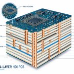
A 10-Layer HDI PCB Board uses laser microvias, blind and buried vias, and sequential lamination to accommodate fine-pitch BGAs, high-speed signals, and dense electronic circuits. It provides more routing options than a conventional 10-layer PCB, but the stackup and via structure must be selected carefully to avoid unnecessary manufacturing complexity.
This guide covers common 10-layer HDI PCB stackups, practical design rules, manufacturing processes, reliability testing, and the factors that affect cost and lead time.
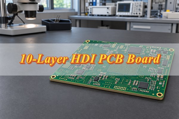
What Are the Common 10-Layer HDI PCB Stackup Structures?
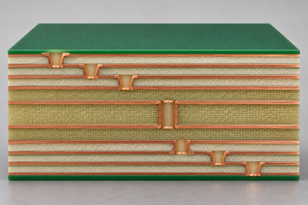
The main 10-layer HDI PCB stackup options are 1+8+1, 2+6+2, and 3+4+3. Each contains ten copper layers, but the number of buildup layers determines the available microvia connections, routing flexibility, and manufacturing complexity.
| Stackup | Construction | Key Advantages | Typical Applications |
|---|---|---|---|
| 1+8+1 | 8-layer core with one buildup layer on each side | Fewer buildup stages and lower manufacturing complexity | Industrial controllers, communication modules, moderate-density BGA designs |
| 2+6+2 | 6-layer core with two buildup layers on each side | More layer-transition options for dense BGA routing | High-density computing, medical electronics, compact communication devices |
| 3+4+3 | 4-layer core with three buildup layers on each side | Additional routing levels for complex interconnections | Space-constrained electronics with demanding BGA fanout |
For most designs, the first decision is whether one or two buildup levels are needed.
A 1+8+1 stackup is suitable when signals can escape the component area through L1–L2 or L10–L9 microvias and reach the required internal layers through the approved core interconnections.
A 2+6+2 structure becomes useful when the available escape channels are insufficient. The additional L2–L3 and L9–L8 transitions allow signals to reach more routing layers without relying entirely on through holes.
A 3+4+3 construction provides another buildup level on each side, but it also introduces more lamination stages and interconnect interfaces.
Start with 1+8+1 and move to a more complex structure only when BGA fanout, routing density, or layer-transition requirements justify the additional buildup layers.
How Do You Choose Materials and Board Thickness for a 10-Layer HDI PCB?
Material selection for a 10-Layer HDI PCB Board depends on its electrical performance, operating temperature, thermal expansion, and required thickness. The laminate must also withstand repeated heating during sequential lamination and PCB assembly.
Common material options include:
- Standard FR-4: Suitable for general industrial electronics, embedded controllers, and other applications where its thermal and electrical properties meet the design requirements.
- High-Tg FR-4: Used for multilayer designs requiring improved thermal stability. Through-thickness expansion and decomposition temperature are important alongside Tg.
- Low-Loss Laminates: Appropriate for high-speed digital and RF circuits where dielectric loss affects signal transmission.
- Hybrid Laminates: Allow different dielectric materials within one construction when electrical requirements vary between circuit layers.
For high-speed applications, dielectric constant (Dk) and dissipation factor (Df) should be selected according to the operating frequency and signal-loss requirements.
Board thickness is determined by the copper layers and dielectric materials throughout the stackup. A 10-layer PCB has nine dielectric separations, leaving less room for each layer when the finished board must be thin.
Several factors influence the thickness design:
- Dielectric Thickness: Affects controlled impedance, insulation, and laser microvia depth.
- Copper Thickness: Determines current capacity, conductor geometry, and contribution to total board thickness.
- Copper Distribution: Balanced copper coverage helps reduce distortion during lamination.
- Thermal Expansion: Material expansion during soldering and operation affects the reliability of plated interconnections.
- Finished Thickness Tolerance: Must account for the pressed dielectric and finished copper dimensions.
Thin 10-layer HDI boards require closer control of dielectric thickness and copper balance. Lighter copper or thinner dielectric layers may be needed, but these changes must still satisfy electrical performance and mechanical requirements.
What Are the Key Design Rules for a 10-Layer HDI PCB?
The key design rules for a 10-Layer HDI PCB Board cover trace geometry, laser microvia dimensions, dielectric thickness, capture pads, copper clearances, and controlled impedance. Establishing these parameters before routing helps avoid designs that require extensive modification during manufacturing review.
| Design Parameter | Typical Reference | Design Recommendation |
|---|---|---|
| Trace Width / Spacing | 0.10/0.10 mm; 0.075/0.075 mm for finer HDI routing | Use wider traces where space allows; reserve finer geometry for dense BGA escape areas |
| Laser Microvia Diameter | 0.10–0.125 mm | Select according to dielectric depth, target pad size, and filling requirements |
| Microvia Aspect Ratio | Preferably ≤0.8:1; 1:1 is the conventional microvia upper limit | Keep the drilled depth low relative to the hole diameter to support reliable metallization |
| Buildup Dielectric Thickness | Commonly 0.06–0.08 mm | Coordinate with laser drilling depth and impedance requirements |
| Microvia Capture Pad | Approximately 0.30 mm for a 0.10 mm microvia as a conservative starting point | Allow sufficient annular ring and layer-registration margin |
| Copper-to-Edge Clearance | 0.25 mm outer-layer and 0.40 mm inner-layer starting allowances for some routed-board processes | Adjust for the actual profiling method, registration, and outline tolerance |
| Controlled Impedance | Common design targets include 50 Ω single-ended and 100 Ω differential | Calculate from finished conductor geometry, dielectric properties, and reference planes |
| Layer Registration | Determined by the selected buildup construction | Maintain adequate alignment allowance for all microvia landing pads |
For example, a 0.10 mm laser microvia drilled through a 0.07 mm dielectric produces a depth-to-diameter ratio of 0.7:1, which is favorable for metallization.
High-speed traces also need continuous reference planes and suitable return-current paths. Impedance values should be calculated using the final stackup rather than selected from nominal trace widths alone.
For designs requiring exceptionally fine traces, small pads, or narrow copper-to-edge clearances, the relevant geometry should be evaluated together with the copper thickness and fabrication method.
How Are Microvias, Blind Vias, and Buried Vias Designed in a 10-Layer HDI PCB?
Microvias, blind vias, and buried vias are arranged according to the required layer connections and available BGA routing space. Their placement determines how signals move from densely populated component pads to the internal signal layers.
The appropriate via structure depends on the selected HDI stackup.
- 1+8+1 Stackup: Laser microvias normally connect L1–L2 and L10–L9. Signals requiring deeper connections can continue through suitable buried vias or plated through holes within the approved construction.
- 2+6+2 Stackup: Microvia transitions can connect L1–L2, L2–L3, L10–L9, and L9–L8. Buried vias may connect selected internal layers within the L3–L8 core.
- 3+4+3 Stackup: Additional buildup levels provide more layer-transition options, but the required microvia arrangement becomes more complex.
For fine-pitch BGA components, microvias can be placed near or inside solder pads to free routing channels. A 0.40 mm pitch BGA, for example, may require microvia-in-pad routing when conventional fanout cannot accommodate the signal count.
Multilevel microvias can be arranged in two ways:
- Staggered Microvias: Adjacent microvias are offset rather than directly stacked. This reduces dependence on vertically aligned interfaces and is generally preferable when sufficient routing space is available.
- Stacked Microvias: Microvias are positioned vertically to save routing space. The underlying microvias require suitable copper filling before subsequent buildup layers are added.
For staggered structures, a hole-to-hole clearance of approximately 0.25–0.30 mm is a conservative design starting point where routing space permits. The final spacing depends on the hole sizes, pad geometry, and approved construction.
Stacked microvias are useful beneath densely populated BGAs, but additional stacked interfaces increase the importance of plating quality and thermal reliability. Direct stacking over buried vias requires careful evaluation.
Via-in-Pad structures also require appropriate filling and surface finishing. Copper-filled microvias are commonly used for HDI BGA pads, while larger mechanically drilled vias may require resin filling and copper capping.
The final via arrangement should provide the required routing access without introducing unnecessary stacked connections or additional buildup levels.
How Is a 10-Layer HDI PCB Manufactured?
A 10-Layer HDI PCB Board is manufactured through inner-layer fabrication, buried-via processing, sequential lamination, laser drilling, copper plating, and final surface finishing. Unlike a conventional multilayer PCB, each HDI buildup level requires a coordinated sequence of lamination and microvia processing.
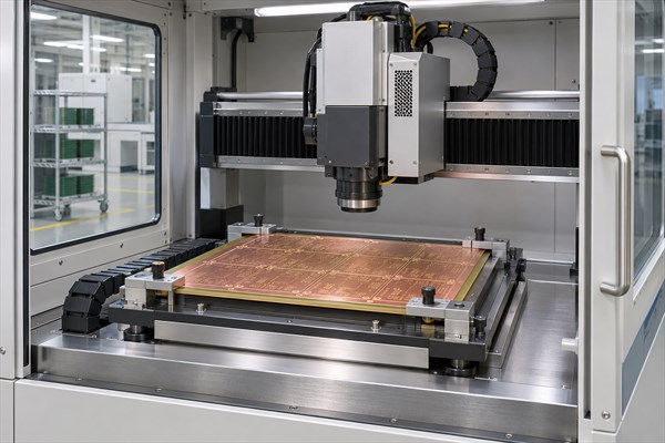
The manufacturing process generally includes:
- Engineering Review: Check the fabrication files, stackup, materials, copper thickness, impedance requirements, and interlayer connections before production.
- Inner-Layer Fabrication: Form the internal copper circuits through imaging and etching. AOI identifies conductor defects before lamination.
- Buried Via Processing: Drill and plate the required internal connections within the core or subassembly. Fill or plug the vias where specified.
- Core Lamination: Align and press the internal layers under controlled temperature and pressure to achieve the required dielectric structure and layer registration.
- Sequential HDI Buildup: Add dielectric and copper layers to the core. A 1+8+1 structure requires one buildup level per side, while a 2+6+2 structure requires two.
- Laser Drilling and Microvia Plating: Drill microvias to the target pads, clean and metallize the holes, and carry out copper filling where required. These operations are repeated for additional buildup levels.
- Outer-Layer Circuit Formation: Complete the outer conductor patterns through imaging, plating, and etching, maintaining the specified fine-line geometry.
- Solder Mask and Surface Finish: Apply solder mask and the specified finish, such as ENIG or ENEPIG, according to the assembly requirements.
- Profiling: Produce the PCB outline using the approved machining method and transfer the finished boards for final inspection.
Sequential lamination requires accurate layer registration, while laser drilling and copper filling must produce reliable connections between buildup levels. These processes are particularly important for 2+6+2 and more complex HDI constructions.
How Is 10-Layer HDI PCB Quality and Reliability Tested?
A 10-Layer HDI PCB Board requires inspection of both the conductor patterns and internal connections. Electrical continuity alone cannot reveal every defect in microvias, buried vias, or laminated structures.
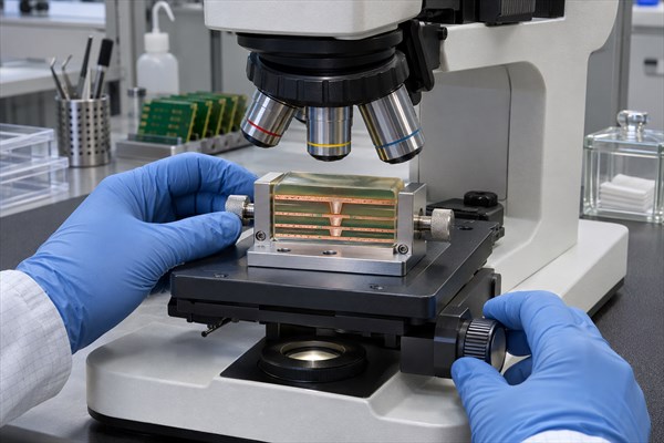
The main quality checks include:
- Automated Optical Inspection (AOI): Detects opens, shorts, incomplete etching, and conductor defects before subsequent processing.
- Electrical Testing: Verifies connectivity and isolation against the approved circuit netlist.
- Microsection Analysis: Examines plating thickness, microvia filling, layer alignment, and interconnect interfaces to identify voids, cracks, or insufficient copper.
- Controlled Impedance Testing: Measures representative test coupons to verify compliance with specified impedance requirements.
- Dimensional Inspection: Checks finished board thickness, hole dimensions, outline geometry, and critical mechanical tolerances.
- Thermal Reliability Testing: Evaluates interconnect stability under temperature changes, particularly for stacked microvias that may develop failures after soldering or thermal cycling.
Applicable IPC-6012 and IPC-A-600 requirements provide acceptance criteria for the specified PCB quality class.
Case Study: Custom 10-Layer HDI PCB Manufacturing Project
EBest Circuit supported the engineering preparation of a 10-layer HDI PCB for an industrial control module destined for Germany. The project involved impedance requirements, resin-plugged vias, and a specified panel layout.
Project Background
The customer needed a compact industrial control PCB with high routing density and defined electrical requirements. The fabrication data required additional clarification before the manufacturing stackup could be finalized.
Project Requirements
- PCB Type: 10-Layer HDI PCB
- Material: FR-4 Tg170
- Finished Thickness: Approximately 1.29 mm ±10%
- Surface Finish: ENIG, with a specified gold thickness of 1 µin
- Via Treatment: Resin plugging and plated-flat processing
- Quality Standard: IPC Class 2
- Panelization: Four boards per panel
- Impedance: Customer-defined requirements requiring clarification
Manufacturing Challenges and Solutions
The main difficulty was aligning the impedance requirements with the manufacturing stackup. Incomplete electrical information could lead to incorrect dielectric thickness or conductor geometry.
EBest Circuit raised engineering queries to clarify the impedance specifications and related stackup details before production release.
The specified resin plugging and plated-flat treatment were also incorporated into the manufacturing instructions. This established the required via-processing conditions for subsequent assembly.
The customer required a four-board panel arrangement, which was retained in the production documentation rather than replaced with an unapproved layout.
Project Results
The engineering review identified the impedance details requiring customer confirmation and established the specified via treatment and panelization requirements for manufacturing-data approval.
The documented work covered engineering preparation and production-data review. Final fabrication and delivery results were not part of the available project record.
What Factors Affect the Cost of a 10-Layer HDI PCB?
The cost of a 10-Layer HDI PCB Board depends on its buildup structure, microvia complexity, materials, conductor geometry, and production quantity. The most significant differences often come from the number of sequential lamination stages and the required via processing.
- Buildup Structure: A 2+6+2 or 3+4+3 stackup requires more manufacturing operations than 1+8+1.
- Microvia Processing: Stacked microvias, copper filling, and high-density via-in-pad layouts add drilling, plating, and inspection operations.
- Materials: Low-loss laminates, specialized dielectrics, and unusual thicknesses can increase material and processing expenses.
- Fine-Line Geometry: Narrow trace widths and spacing require greater precision during imaging and etching.
- Mechanical Requirements: Tight outline tolerances and thin constructions may increase machining and handling difficulty.
- Production Quantity: Prototype orders carry higher engineering and setup expenses per board, while larger quantities can improve manufacturing efficiency.
Cost can be reduced by selecting the simplest stackup that meets the routing requirements, limiting stacked microvias to necessary locations, and avoiding unnecessarily tight tolerances.
What Is the Lead Time for 10-Layer HDI PCB Prototypes and Mass Production?
The lead time for a 10-Layer HDI PCB Board depends on the buildup structure, material availability, microvia processing, testing requirements, and order quantity.
For HDI prototype planning, EBest Circuit generally uses approximately 2.5–3.5 weeks as a reference for 1+N+1 and 2+N+2 constructions. Actual schedules depend on the approved design and production requirements.
- Prototype Production: Lead time is influenced by stackup approval, material availability, and the required HDI processes.
- Small-Batch Production: Scheduling depends on panel quantity, production capacity, and inspection scope.
- Mass Production: Material planning, manufacturing capacity, and batch quality control determine the production schedule.
- Expedited Production: Shorter lead times may be available when materials, process complexity, and equipment capacity allow.
A 1+8+1 design generally requires fewer buildup operations than a comparable 2+6+2 construction. Special materials, additional qualification tests, or complex via structures may extend the manufacturing schedule.
Manufacturing lead time begins after production-data approval and excludes international shipping and customs clearance.
Why Choose EBest Circuit for 10-Layer HDI PCB Manufacturing?
EBest Circuit provides 10-Layer HDI PCB fabrication, engineering support, and PCB assembly services, helping you resolve design issues, control manufacturing quality, and move from prototypes to volume production.
- Free DFM and Engineering Support: Get a free review of your stackup, microvia layout, impedance requirements, and material selection, with practical recommendations to address manufacturing risks before production.
- Custom HDI PCB Manufacturing: Order 1+8+1, 2+6+2, and other custom HDI constructions with blind and buried vias, laser microvias, and fine-line routing to meet your project requirements.
- Prototype to Mass Production: Build engineering samples, verify your design, and transition to volume manufacturing with consistent specifications and coordinated production planning.
- One-Stop PCB Assembly: Combine PCB fabrication with component sourcing, SMT assembly, and functional testing through one supplier, reducing communication and coordination between separate providers.
- Quality Assurance and Delivery Support: Access electrical testing, impedance verification, and applicable quality documentation, supported by ISO 9001, ISO 13485, IATF 16949, and AS9100D quality management systems. Receive engineering assistance and project-specific production scheduling.
FAQ About 10-Layer HDI PCB Boards
Q1: What Is the Difference Between IPC Class 2 and Class 3 for a 10-Layer HDI PCB?
A1: IPC Class 2 applies to dedicated-service electronic products, while Class 3 covers high-performance applications requiring stricter acceptance criteria. The required class should be specified in the fabrication documentation.
Q2: Can ENEPIG Be Used Instead of ENIG on a 10-Layer HDI PCB?
A2: Yes. Both surface finishes support soldering, while ENEPIG can also be suitable for certain wire-bonding applications. Selection depends on the assembly process and pad-finish requirements.
Q3: Can a 10-Layer HDI PCB Use Through-Hole Connectors and Fine-Pitch BGAs Together?
A3: Yes. Plated through-hole connectors can be combined with HDI interconnections. Connector hole dimensions, clearances, and assembly requirements must be included in the design.
Q4: Can Components Be Assembled on Both Sides of a 10-Layer HDI PCB?
A4: Yes. Double-sided SMT assembly is possible when component placement, soldering profiles, and board support are properly planned.
Q5: Can a 10-Layer HDI PCB Include Hard Gold Edge Connectors?
A5: Yes. Selective hard gold plating can be used for edge contacts. Plating thickness, contact geometry, and beveling requirements must be specified.
Q6: Are Fiducials and Tooling Holes Required on HDI PCB Assembly Panels?
A6: Automated assembly commonly uses fiducials for alignment and tooling holes for panel handling. Their dimensions depend on the assembly process.
Q7: Can the PCB Design Be Revised After Prototype Approval?
A7: Yes. Revised fabrication files must be reviewed before further production. Changes to interconnections, component pads, or manufacturing requirements may require additional verification.
Q8: Can Different 10-Layer HDI PCB Designs Be Combined in One Panel?
A8: Mixed-design panels may be possible when the boards use compatible materials, layer structures, thicknesses, and manufacturing processes.
Q9: Can an NDA Be Signed Before Submitting HDI PCB Design Files?
A9: Confidentiality requirements can be discussed with EBest Circuit before transferring sensitive design files. NDA terms, authorized access, and file-retention arrangements should be agreed upon in advance.
How Can You Get a Custom 10-Layer HDI PCB Quote?
EBest Circuit provides custom 10-Layer HDI PCB Board manufacturing, prototype fabrication, engineering support, and optional PCB assembly services. Send your Gerber or ODB++ files, stackup drawing, material specifications, copper requirements, via details, order quantity, required delivery date, and delivery location to sales@bestpcbs.com. Our engineering team can review your manufacturing requirements and provide technical recommendations, a project-specific quotation, and a production plan for your 10-layer HDI PCB project.
You may also like






Tags: 10-Layer HDI PCB Board, 10-Layer HDI PCB Stackup, HDI PCB Design Rules, HDI PCB Manufacturing Process