

PCB bus bar is a proven power distribution solution in modern power electronics, designed to carry high current with lower resistive loss, reduced thermal buildup, and minimal voltage drop compared to traditional copper traces. This article explains what high-current PCB bus bars are, how different bus bar structures function in power designs, and which manufacturing capabilities are required to produce them reliably, while highlighting how professional PCB bus bar manufacturing directly impacts system efficiency, thermal stability, and long-term reliability.
EBest Circuit (Best Technology) supports customers throughout the entire lifecycle of solderable PCB bus bars projects—from R&D design and engineering validation to rapid industrialization and production ramp-up. Driven by a strong sense of commitment, our team demonstrates a high level of professionalism and dedication in delivering high-quality, one-stop PCBA services. The United States, Germany, and Israel ranked as our top three export markets in the past year, reflecting long-term trust from global customers. To date, we have served more than 10,000 engineers and 1,800 customers worldwide.
Guided by a common vision of responding precisely to customer requirements, we focus on delivering reliable solutions that meet real high-current application needs. If you have any requirements for high current busbar PCB, please feel free to contact us at sales@bestpcbs.com.
What Is a PCB Bus Bar and Why Is It Used in Power Electronics?
A PCB bus bar is a solid conductive structure—typically copper—integrated into or mounted onto a PCB to distribute high current efficiently. It replaces or supplements wide copper traces when current levels exceed what standard PCB routing can safely support.
From an engineering perspective, power electronics systems such as inverters, converters, EV power modules, and industrial drives demand low impedance paths with predictable thermal behavior. PCB bus bars provide controlled cross-sectional area, uniform current flow, and improved heat dissipation compared to etched copper alone.
In real-world power designs, bus bars are used to stabilize voltage under load, reduce EMI caused by uneven current density, and extend product lifespan. As a result, PCB bus bars have become a standard element in high-power PCB architecture rather than a niche solution.
How Do PCB Bus Bars Improve High Current Handling Compared to Copper Traces?
High-current applications quickly expose the limitations of conventional PCB copper traces. Even with heavy copper, etched traces are constrained by foil thickness, heat concentration, and PCB dielectric limits, making them unsuitable for sustained high current paths.
PCB bus bars overcome these constraints by introducing solid copper conductors with controlled geometry, significantly reducing resistance and thermal rise. From an engineering perspective, this shift is not incremental—it fundamentally changes how current is distributed across the board.
In real power electronics builds, engineers typically observe lower voltage drop, more stable thermal behavior, and reduced risk of copper delamination once bus bars replace wide copper pours. The difference becomes especially clear when current levels exceed the safe operating range of standard PCB copper.
| Parameter | Standard Copper Trace | PCB Bus Bar |
|---|---|---|
| Typical Current Capacity | Limited by copper weight | 50–300A |
| Conductor Thickness | ≤ 6 oz copper foil | 1.0–3.0 mm solid copper |
| Voltage Drop | Higher under load | Significantly lower |
| Thermal Dissipation | Relies on PCB laminate | Improved via copper mass |
| Mechanical Strength | Low | High, load-bearing |
| Long-Term Reliability | Moderate at high current | Excellent for power electronics |
As a result, PCB bus bars are no longer viewed as optional enhancements but as essential structures once power density and current levels rise beyond standard PCB limits.
What Types of PCB Bus Bars Are Commonly Used in Power Designs?
PCB bus bars come in multiple structural forms, selected based on current level, mechanical constraints, and assembly method.
Common types include:
- Surface-mounted bus bars soldered or bolted onto the PCB
- Through-hole copper bus bars mechanically fixed and soldered
- Embedded bus bars laminated inside the PCB stackup
- Hybrid bus bar structures combined with thick copper layers
In practice, surface-mounted bus bars are widely used for flexibility, while embedded bus bars are favored in compact, high-density power modules. From an engineering perspective, selecting the right structure early prevents layout rework later.
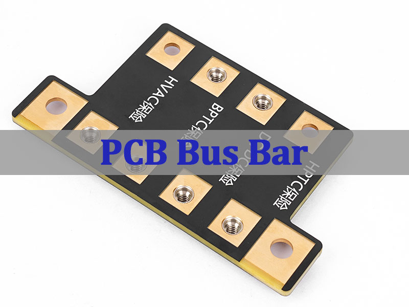
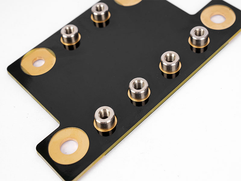
How Are Solderable PCB Bus Bars Integrated into PCB Assemblies?
Solderable PCB bus bars are designed to be assembled using controlled soldering processes while maintaining mechanical stability. Their integration must account for solder volume, wetting behavior, and thermal expansion.
From a manufacturing standpoint, these bus bars require:
- Precisely defined solder pads
- Controlled solder thickness
- Stable fixturing during reflow or selective soldering
In real assembly lines, improper soldering can lead to voids, weak joints, or stress cracking. Professional PCBA processes ensure repeatable joints even under high thermal cycling. That said, solderable bus bars must always be treated as load-bearing conductors, not standard SMT components.
What Is a Bus Bar Embedded PCB and When Should It Be Used?
A bus bar embedded PCB integrates a solid copper conductor directly into the PCB during lamination. This approach shortens current paths and improves thermal coupling.
From a design perspective, embedded bus bars are ideal when:
- Space is limited
- Current levels are extremely high
- Thermal control is critical
In real products such as EV power control units or industrial power modules, embedded bus bars reduce inductance and improve system stability. In practice, this solution requires close coordination between design and manufacturing from the earliest stage.
Why Is Copper Bus Bar for PCB Critical in High-Power Applications?
A copper busbar for PCB is essential because busbar copper offers unmatched electrical conductivity and predictable thermal behavior under continuous load.
Engineering analysis shows that copper bus bars:
- Lower I²R losses
- Distribute heat more evenly
- Reduce voltage drop across power paths
In production environments, copper bus bars also improve long-term reliability by reducing stress on solder joints and PCB dielectric materials. More importantly, copper bus bars allow power electronics to operate closer to design limits without sacrificing safety margins.
How Does PCB Power Bus Bar Design Affect Reliability and Thermal Performance?
PCB power bus bar design directly influences system reliability. Geometry, mounting method, and surface finish all impact electrical resistance and heat dissipation.
Key design considerations include:
- Cross-sectional area sized for continuous current
- Short, direct routing paths
- Mechanical anchoring to prevent vibration damage
- Thermal interfaces to heatsinks or copper planes
In real operation, poorly designed bus bars become failure points. Well-designed bus bars, however, stabilize both electrical and thermal behavior over the product lifetime. Ultimately, bus bar design is a reliability decision, not just a current-rating exercise.
What Manufacturing Capabilities Are Required for Power Bus Bar PCB Production?
Manufacturing a power bus bar PCB requires capabilities well beyond conventional PCB fabrication. Precision copper handling, structural control, and process discipline determine whether a bus bar PCB performs reliably or becomes a failure point under load.
From a production standpoint, bus bar PCBs must balance electrical performance, mechanical integrity, and manufacturability. This demands tight control over copper spacing, thickness, drilling quality, and surface finishing—all executed within a coordinated PCB + PCBA workflow.
In real manufacturing environments, insufficient capability often results in uneven current distribution, assembly difficulty, or long lead-time delays. Professional manufacturers address these risks through standardized parameters and proven process windows.
| Manufacturing Parameter | Typical Capability for Bus Bar PCB |
|---|---|
| Copper Bar Thickness | 1.0–3.0 mm |
| Current Carrying Capacity | 50–300A |
| Minimum Copper Bar Spacing | 0.8–1.0 mm |
| Board Thickness | 3.0–6.0 mm |
| Hole Wall Copper Thickness | ≥ 25 μm |
| Thickness-to-Diameter Ratio | 1:6 or 1:7 |
| Layer Count | 3–4 layers typical (expandable) |
| Surface Finishes | ENIG, Immersion Silver, Gold Plating |
| Maximum PCB Size | 600×400 mm (standard), 900×600 mm (double-sided) |
| Lead Time | 13–15 days (3–4 layers) |
These capabilities ensure that power bus bar PCBs behave predictably under electrical and thermal stress while remaining compatible with downstream assembly processes.
All things considered, power bus bar PCB production is less about speed and more about executing every parameter within a controlled, repeatable manufacturing framework.
Why Choose a Professional PCB Bus Bar Manufacturer for Power Electronics Projects?
Choosing a professional PCB bus bar manufacturer directly impacts product performance and risk. At EBest Circuit (Best Technology), we approach bus bar manufacturing as a system-level engineering task.
Our strengths include:
- Integrated PCB fabrication and PCBA assembly
- Experience with high-current and power electronics designs
- Engineering-led DFM review for bus bar integration
- Controlled processes for repeatable power performance
Rather than treating bus bars as accessories, we design and manufacture them as core power components. Fundamentally, this approach reduces failure risk and accelerates qualification for power electronics products.
In a nutshell, PCB bus bar solutions enable stable, high-current power distribution where traditional PCB copper reaches its limits. This article explained how bus bars function, how different structures are used, and why manufacturing capability determines performance. EBest Circuit (Best Technology) delivers professional bare copper busbar PCB manufacturing with engineering discipline, integrated production, and proven reliability for power electronics projects. For technical consultation or quotations, please contact us via sales@bestpcbs.com.
FAQ: PCB Bus Bar
Q1: What current levels can a PCB bus bar safely handle?
PCB bus bars can support tens to hundreds of amperes depending on copper thickness, geometry, and thermal design.
Q2: Are PCB bus bars better than thick copper PCBs for power distribution?
Yes. Bus bars offer lower resistance and better thermal stability than thick copper alone in high-current applications.
Q3: Can PCB bus bars be used with SMT and through-hole assembly?
Yes. Bus bars can be integrated with SMT, THT, or mixed assembly depending on design requirements.
Q4: How early should PCB bus bars be considered in power PCB design?
They should be considered during initial schematic and layout planning to avoid redesign and thermal issues later.
Tags: Bus Bar Embedded PCB, Copper Bus Bar for PCB, PCB Bus Bar, PCB Bus Bars, PCB Power Bus Bar, Power Bus Bar PCB, Solderable PCB Bus Bars