

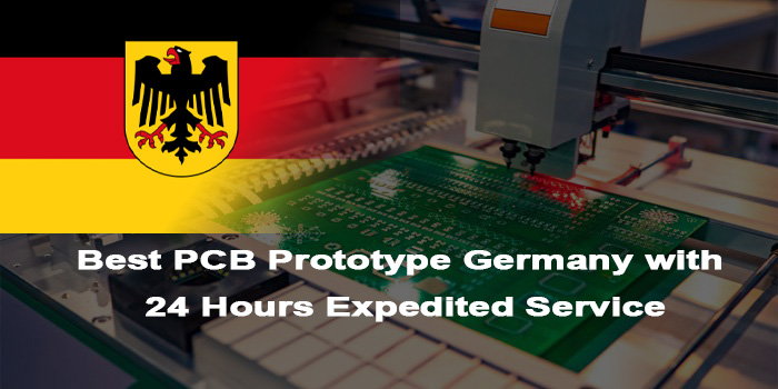
High-quality PCB prototype Germany plays a critical role in accelerating electronic project timelines, blending precision engineering with on-time delivery. Our PCB prototype Germany services meet the varied requirements of multiple industries, using cutting-edge technologies to produce reliable prototypes compliant with stringent European norms.
Why Choose PCB Prototype Germany?
Advantages of PCB Prototype Company:
- Precision Manufacturing: Adheres to rigorous German engineering standards, ensuring trace widths down to 50 µm and consistent board thicknesses from 0.4 mm to 7.0 mm.
- Localized Support: Proximity enables faster communication, reduced shipping delays, and compliance with regional regulations like RoHS and WEEE.
- Quality Material Sourcing: Uses premium materials from trusted brands like Panasonic and Nanya, including halogen-free high-Tg substrates for durability.
- Year-Round Reliability: Delivers consistent production even during international holidays, avoiding disruptions to project timelines.
- Technical Versatility: Supports complex processes such as HDI microvia, impedance control, and semi-flex deep milling for diverse applications.
Top 10 Best PCB Prototype Germany Manufacturer
| Company Name | Main Business | Core Advantages | Process Capabilities | Prototyping Lead Time |
| EBest Circuit Co., Limited | PCB prototype, manufacturing, PCBA one-stop service | 20-year experience, 99.8% yield rate, MES traceability | 2-20 layers, HDI (0.1mm microvias), ceramic boards | 24hrs (2-4 layers), 72hrs (HDI) |
| Schweizer Electronic AG | Embedded packaging PCB, high-reliability circuit boards | Founded 1849, European top 3 PCB maker | 2-16 layers, embedded components | 3-5 days (standard) |
| Weidmüller Group | Industrial-grade PCB, PCB connectors | UL/CSA certified, 80+ countries network | 2-8 layers, industrial-grade finishes | 4-6 days (standard) |
| Beta Layout GmbH | Rapid PCB prototyping, RFID-integrated PCB | UL certified Magic-PCB technology | 2-10 layers, RFID-embedded PCB | 2-3 days (standard) |
| Zollner Elektronik AG | High-reliability PCB, PCBA services | Automotive/aviation certification | 2-24 layers, HDI blind/buried vias | 5-7 days (standard) |
| Phoenix Contact GmbH | Industrial PCB, automation-related boards | ISO 9001 certified, 100+ years experience | 2-6 layers, anti-vibration design | 6-8 days (standard) |
| Würth Elektronik | RF/microwave PCB, passive components | IATF 16949 automotive certification | 2-12 layers, RF impedance control | 4-5 days (standard) |
| AT&S Austria (German Branch) | High-density HDI PCB, automotive boards | HDI technology leader | 4-20 layers, HDI blind/buried vias | 5-7 days (standard) |
| Eurocircuits GmbH | Prototype & small-batch PCB | Pan-European production network | 2-16 layers, rigid-flex PCBs | 3-4 days (standard) |
| HARTING Electronics | Heavy-duty industrial PCB | IP67 protection grade support | 2-8 layers, anti-corrosion design | 7-10 days (standard) |
Pain Points of PCB Prototype Germany
- High small-batch costs due to fixed engineering and photomask fees for low-volume orders.
- Prolonged lead times for complex HDI or ceramic board prototypes delay project launches.
- Limited supply of specialized substrates restricts high-temperature and high-frequency applications.
- Inconsistent quality across suppliers causes repeated testing failures and rework expenses.
- Lack of integrated PCBA services increases vendor coordination and logistical complexity.
- Poor production transparency makes prototype progress tracking difficult.
- Expedited services are overpriced, exceeding tight project budgets.
Why Choose EBest(Best Technology) for PCB Prototyping Germany?
Reasons Why Choose EBest(Best Technology) for PCB Prototyping Germany:
- 24-Hour Rapid Prototyping Expedited Service: Deliver high-precision prototype PCB Germany for 2-4 layer boards in just 24 hours, 70% faster than local industry averages. No compromise on precision for speed, ensuring projects stay ahead of tight launch timelines.
- 19+ Years of Industry Expertise: Boast a 99.2% on-time delivery rate for PCB prototyping Germany across 1000+ high-demand projects. Our deep understanding of German industrial standards ensures seamless alignment with local requirements.
- Advanced Process Capabilities: Master complex manufacturing like ceramic boards (200 W/m·K thermal conductivity) and HDI with 0.1mm microvias, filling the gap of specialized substrate supply in local PCB prototype Germany market.
- Strict Quality Assurance: Hold ISO9001, AS9100D, and IATF 16949 certifications, guaranteeing a 99.8% prototype yield rate. Surpass local quality inconsistencies with rigorous multi-stage testing for reliability.
- One-Stop PCBA Solution: Integrate PCB production and assembly to cut project time by 30%, eliminating the hassle of coordinating multiple vendors and reducing logistical complexity.
- MES-Enabled Full Traceability: Real-time production tracking from material sourcing to shipment via MES system, solving poor transparency issues common in PCB prototyping Germany and keeping you in full control.
- Cost-Effective Expedited Service: Offer expedited fees 20% lower than German local competitors, making fast turnaround accessible even for tight-budget projects without sacrificing quality.
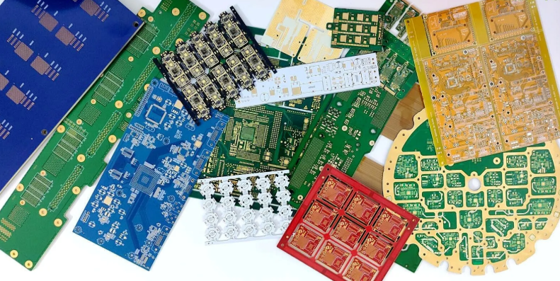
Custom PCB Prototype Germany Services We Offer
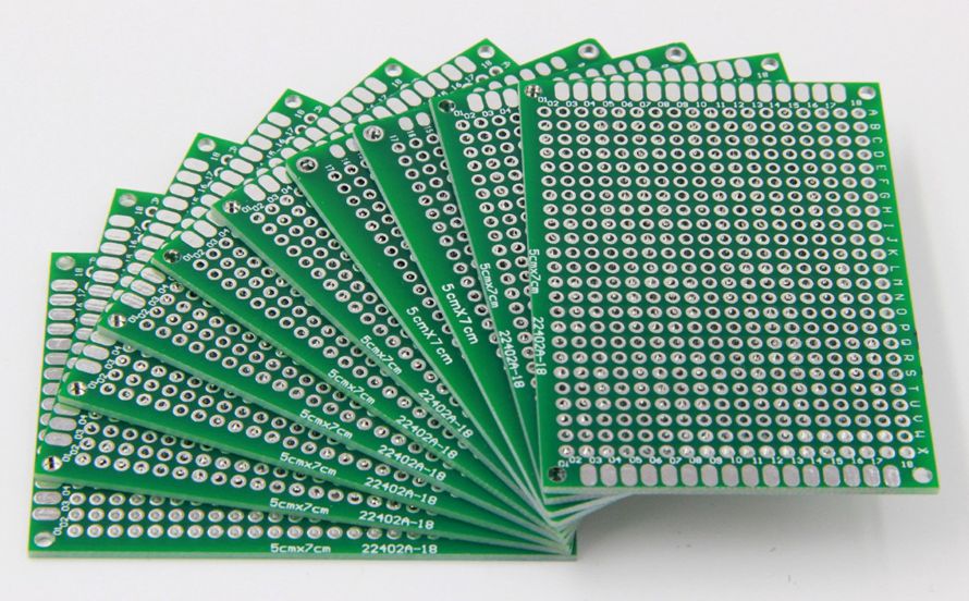
- Rigid PCB Prototypes: 2-16 layers, 0.4-7.0mm thickness, HASL/ENIG surface finishes, RoHS compliant.
- Flexible & Semi-Flex Prototypes: Polyimide substrates, precise deep milling, suitable for compact devices.
- HDI PCB Prototypes: Up to 20 layers, blind/buried vias, ideal for high-density electronic products.
- Ceramic PCB Prototypes: High-temperature resistance, 200 W/m·K thermal conductivity for industrial use.
- Metal Core Prototypes: Aluminum/copper core for thermal management in automotive projects.
- RF & Microwave Prototypes: ±5% impedance tolerance, supporting wireless communication devices.
Our Quality Standards for Prototype PCB
- Material Compliance & Grade Assurance: All substrates are 100% RoHS 2.0 compliant, adhering to restrictions on 11 hazardous substances (each ≤0.1%). We follow IPC-A-600 Class 2 and Class 3 standards — Class 2 for general electronics with acceptable minor defects, and Class 3 for high-reliability PCB prototype Germany in medical/automotive sectors (zero critical defects). This ensures smooth European market certification and avoids compliance delays.
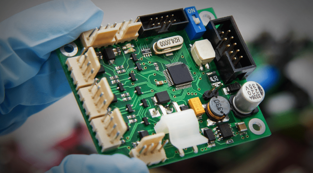
- Full-Coverage Electrical Testing: Every prototype undergoes 100% electrical testing via Keysight E4980A LCR meters. We verify continuity, insulation resistance (>10?Ω at 500V DC) and impedance (±5% tolerance for 50Ω/75Ω standards). Ansys SIwave pre-production simulation identifies signal integrity risks upfront, cutting rework costs by up to 40%.
- High-Precision Visual & Automated Inspection: AOI inspection uses Koh Young Zenith 3D equipment (20μm resolution, 30cm?/sec speed) to detect soldering bridges, component offset (≤0.05mm), surface scratches (<0.1mm) and solder paste inconsistencies. Critical prototype PCB Germany for medical use gets 100% manual recheck by senior technicians (5+ years of experience), achieving 99.9% defect detection.
- Premium Substrate & Traceability: We standardize on halogen-free high-Tg (≥170℃) substrates (Panasonic R-1766, Nanya NE-160A) and offer AlN ceramic substrates (200 W/m·K thermal conductivity) for high-heat needs. Each batch has manufacturer certification, with MES system tracking substrate lot numbers, production timelines and test data for full traceability.
- Industrial-Grade Environmental Validation: Prototypes undergo IPC-6012/2221 testing, including 1000 cycles of temperature cycling (-40℃ to 125℃ at 5℃/min) and 1000 hours of 85℃/85%RH humidity aging. Post-test inspection confirms substrate warpage (≤0.2%) and impedance drift (<3%), ensuring stability for PCB prototyping Germany in harsh environments.
Our Lead Time for Germany PCB Prototyping
| Layers | Normal Service | Fastest Service |
| 1 | 7 Days | 24 H |
| 2 | 8 Days | 24 H |
| 4 | 10 Days | 48 H |
| 6 | 10 Days | 72 H |
| 8 | 12 Days | 72 H |
| ≥10 | TBD | TBD |
Case Studies of Our Medical PCB Prototyping Germany
Project Background: A German medium-sized professional medical device manufacturer needed prototyping PCB Germany for a portable blood glucose monitor, designed for outpatient rapid testing. The project demanded extreme reliability to avoid misdiagnosis risks and strict compliance with European medical device regulations.
Project Requirements: 6-layer HDI PCB with 0.15mm microvias (blind-buried via interleaving layout), biocompatible ENIG finish (nickel layer 50-100 microinches, gold layer 2-5 microinches), ISO 13485 compliance covering design control and material traceability, and 5-day delivery to meet clinical trial scheduling.
Project Challenges: The 5-day timeline clashed with complex HDI blind-buried via layout; biocompatibility required zero sensitization risk for skin-contact areas; 99.9% electrical reliability mandated signal stability under frequent outpatient use; and full material traceability was needed for ISO 13485 audit.
Our Solutions: Leveraging our PCB prototype Germany expertise, we activated MES system’s medical emergency order channel to prioritize production and sync progress in real time. We adopted medical-grade ENIG materials and Panasonic R-1766 high-Tg substrate, conducted 3 rounds of impedance testing with Keysight E4980A (±5% tolerance), and assigned a team of HDI specialists and medical PCB auditors for full-process coordination.
Output Results: Delivered 50 prototypes in 4 days (20% faster than required) with 99.92% yield rate. All units passed biocompatibility testing and ISO 13485 audit. The client completed clinical trials on schedule, with feedback noting “prototypes maintain signal stability in 1000+ consecutive tests, meeting medical precision demands,” and signed a 3-year contract with annual PCB prototype Germany supply exceeding 500 units.
FAQs of PCB Prototyping Germany
Q1: How to avoid narrow drilling breakage in PCB prototype design?
A1: Adopt high-mechanical-strength substrates like Panasonic high-Tg materials and precision drilling equipment with ±0.01mm tolerance. We support 0.1mm drill sizes for PCB prototype Germany, complemented by 100% plated-through hole inspection to ensure conductivity and eliminate breakage risks.
Q2: What causes inconsistent surface finishes in prototype PCBs?
A2: Inconsistencies arise from improper material storage or uneven plating current. Our process uses climate-controlled storage and automated plating systems, delivering uniform HASL/ENIG finishes for all PCB prototyping Germany orders with 100% visual inspection and AOI verification.
Q3: Can via-filling be added to rapid PCB prototyping orders?
A3: Yes. We provide epoxy via-filling (conductive/non-conductive) for rapid prototyping PCB Germany, which boosts structural stability. This service is available for 24-hour expedited orders without extending lead time, aligning with tight project schedules.
Q4: How to resolve impedance control deviations in high-frequency prototypes?
A4: Optimize trace width and spacing via 3D field simulation tools, paired with precision etching (±5% tolerance). For PCB prototype Germany, we conduct pre-production impedance testing with Keysight equipment and adjust designs to meet 50Ω/75Ω standard values, ensuring signal integrity.
Q5: Why does substrate warpage occur in high-temperature PCB prototypes?
A5: Warpage results from mismatched thermal expansion coefficients of substrate materials and inadequate curing processes. For PCB prototype Germany, we use high-Tg (≥170℃) substrates and precise thermal curing control, followed by post-production flatness testing (≤0.2% warpage) to ensure stability in high-temperature scenarios.
Tags: PCB prototype Germany, PCB prototyping Germany, prototype PCB Germany, prototyping PCB Germany