

Struggling with PCB troubleshooting? Our definitive guide reveals the tools, techniques, and real-world case studies to diagnose and fix any board.
What Tools Are Required for PCB Troubleshooting?
The table below lists the necessary tools and their main uses to help you build a reliable PCB troubleshooting toolkit.
| Tool Name | Purpose |
| Multimeter | Voltage/resistance measurement |
| Soldering Station | Component replacement/repair |
| Oscilloscope | Signal integrity analysis |
| Logic Analyzer | Digital circuit debugging |
| Thermal Camera | Hidden short detection |
| X-ray Inspection | Via/solder joint analysis |
| Tweezers | Precision component handling |
| Magnifying Glass | Visual inspection of solder joints |
| Jumper Wires | Circuit bypass/signal injection testing |
| ESD-Safe Tools | Static protection during handling |
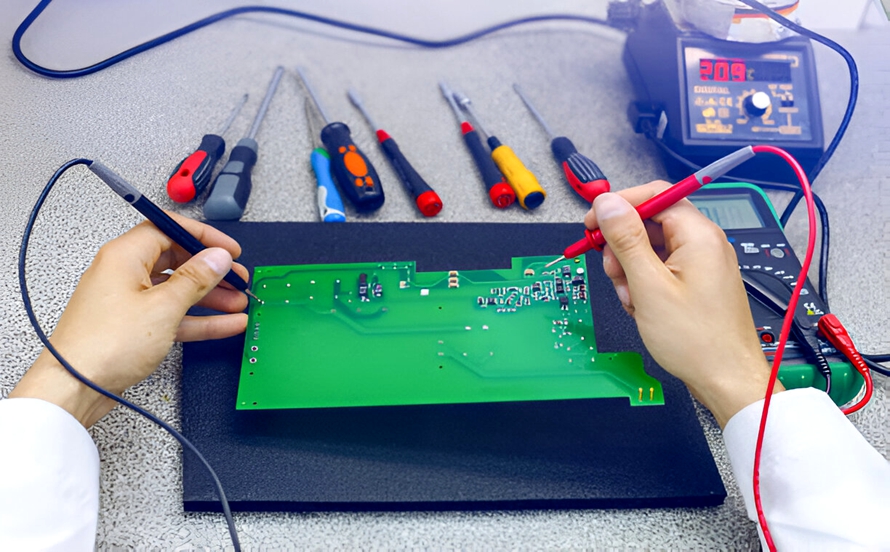
How to Troubleshoot a Circuit Board with a Multimeter?
The digital multimeter (DMM) is the most versatile tool for PCB troubleshooting, and mastering its use can resolve 70% of common board issues. Below is a step-by-step guide to using a multimeter for troubleshooting PCB circuit board problems, from basic continuity checks to component testing.
1. Disconnect Power: Ensure the circuit board is powered off and capacitors are discharged. Safety first—avoid live measurements unless testing in-circuit voltage rails.
2. Set Multimeter to DC Voltage: Configure the multimeter to the appropriate DC voltage range (e.g., 20V scale for logic circuits). Use auto-ranging meters for flexibility.
3. Check Power Rails: Probe VCC and GND points to verify power delivery. A stable 5V/3.3V reading confirms functional power regulation. Deviations indicate regulator or capacitor issues.
4. Test Component Voltage: Measure voltage at critical components (IC pins, resistors) to identify unexpected drops. For example, a 0V reading at a microcontroller’s VCC pin suggests a broken trace or faulty regulator.
5. Continuity Test: Switch to beep/continuity mode to check for open/short circuits. Test traces between components, silence indicates a break, while a beep confirms connectivity.
6. Resistance Measurement: Verify resistor values with the ohms function. Compare measured values to datasheet specs. Unusually high/low readings indicate damaged components.
7. Diode Test: Use the multimeter’s diode mode to confirm proper diode function. A forward voltage drop of ~0.7V (silicon) or ~0.3V (germanium) indicates health. Reverse polarity should show “OL” (open circuit).
8. Document Findings: Record all measurements systematically. Track voltage readings, continuity checks, and resistance values to isolate faults and share results with teams.

PCB Troubleshooting Techniques
Beyond tool use, effective PCB troubleshooting relies on systematic techniques that eliminate guesswork. These methods help isolate problems quickly, whether you’re dealing with a simple hobby board or a complex industrial PCB.
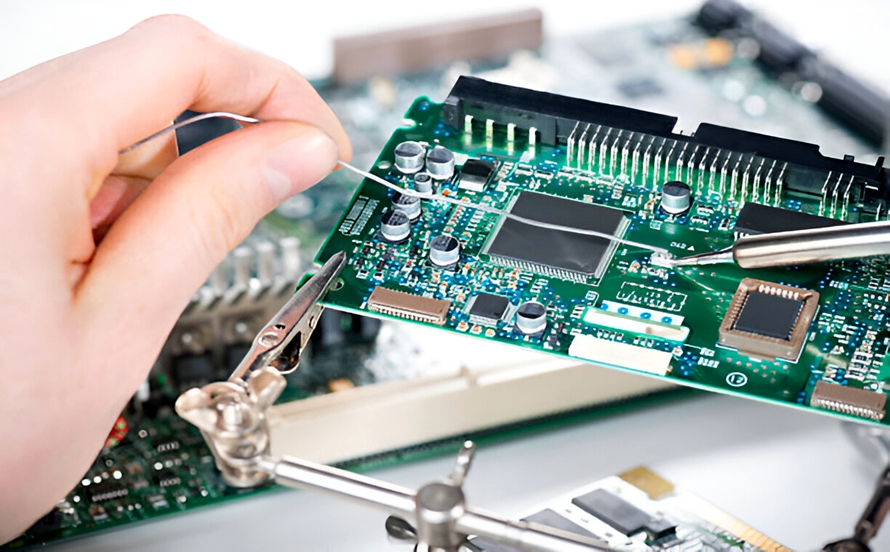
Visual Inspection First
- Before using any tools, perform a thorough visual check, many defects are visible to the naked eye (or with a microscope). Look for: burnt components (charring or discoloration), cold solder joints (dull, grainy appearance), bent pins on ICs, corrosion (common in humid environments), and loose components. This step is often overlooked but can save hours of troubleshooting PCB circuits unnecessarily.
Divide and Conquer Method
- For complex PCBs, split the circuit into smaller, manageable sections (e.g., power supply, input module, output module). Test each section individually to identify which part is malfunctioning. For example, if the PCB won’t power on, first test the power supply section, if it’s working, move to the next section. This technique streamlines PCB troubleshooting by narrowing the focus.
Signal Tracing with an Oscilloscope
- When dealing with intermittent issues or signal distortion, an oscilloscope is invaluable. Trace the signal from the input to the output of the circuit. Compare the actual signal to the expected signal (from the schematic). Anomalies like delayed signals, noise, or clipping will point to the faulty component or trace. This method is particularly effective for troubleshooting pcb circuit board used in high-frequency applications (e.g., communication devices).
Swap Test for Suspected Components
- If you suspect a specific component (e.g., a microcontroller or capacitor) is faulty, replace it with a known-good component of the same specification. This “swap test” is quick and effective, but ensure you use the correct replacement to avoid further damage. Always document which components you swap, this helps with future PCB troubleshooting if similar issues arise.
PCB Board Troubleshooting Case Studies
Project Requirement: Isolate and resolve a persistent short circuit between the 3.3V power plane and ground in a 6-layer PCB (dimensions: 200mm × 150mm) causing intermittent system crashes during thermal stress testing.
Troubleshooting Plan:
- Initial Inspection: IR thermal imaging revealed localized hotspots (ΔT = 18°C above ambient) at via #A12, indicating abnormal current leakage.
- Continuity Testing: Multimeter measurements showed 0.03Ω resistance between power/ground traces at via #A12—significantly lower than the design specification of >100MΩ.
- X-Ray Analysis: 3D X-ray microscopy quantified a 15μm copper bridge between adjacent vias, validated via slice-and-view SEM at 5000× magnification.
- Simulation Verification: Ansys Icepak thermal simulation confirmed a 22% higher current density at via #A12 under peak load, correlating with field failure data.
- Failure Replication: Accelerated life testing (1000 thermal cycles from -40°C to 125°C) reproduced failures exclusively at via #A12, confirming root cause.
Output Result:
- Isolation: Laser-cut precision ablation removed the 15μm copper bridge, verified via post-repair continuity tests (resistance >1GΩ).
- Validation: Post-repair thermal imaging showed normalized temperature distribution (ΔT < 5°C), and functional testing confirmed 100% recovery with zero failures over 5000 thermal cycles.
- Design Improvement: Implemented via-to-plane spacing optimization (increased from 0.2mm to 0.3mm) and added solder mask webbing, reducing short-circuit risk by 92% in subsequent prototypes.
PCB Troubleshooting and Defect Analysis
Open Circuits
- Cause: Incomplete etching, wire/pad fractures, or via misalignment.
- Fix: Use flying probe testing to locate breaks; validate etching parameters and material integrity.
Short Circuits
- Cause: Conductive debris, solder bridge formation, or layer-to-layer misalignment.
- Fix: Conduct electrical testing and X-ray/AOI inspection; clean surfaces and optimize solder mask application.
Solder Joint Defects
- Cause: Poor wetting, insufficient/excess solder, thermal stress, or pad lift-off.
- Fix: Refine reflow profile, ensure pad design meets IPC standards, and validate component alignment.
Layer Registration Issues
- Cause: Imprecise layer stacking or drill misalignment during lamination.
- Fix: Verify registration marks via optical measurement; recalibrate drilling/laminating equipment.
Delamination/Blistering
- Cause: Moisture ingress, inadequate lamination pressure/temperature, or contaminated prepreg.
- Fix: Improve storage conditions, validate lamination parameters, and audit material quality.
Via Defects (e.g., Necking, Resin Starvation)
- Cause: Inadequate plating, drill debris, or void formation.
- Fix: Implement via plugging processes; optimize plating chemistry and drilling parameters.
How to Prevent PCB Board Troubleshooting?
The best PCB troubleshooting is the kind you don’t need to do. Preventive measures during design, manufacturing, and maintenance can significantly reduce the risk of PCB failures. Below are key strategies to minimize troubleshooting PCB efforts.
Robust PCB Design
- Design flaws are a major cause of PCB failures. Use design rules to avoid common issues: ensure adequate trace width for current requirements (thinner traces overheat), place heat-sensitive components away from high-power devices, and include test points for easy PCB troubleshooting (e.g., at key nodes like power inputs and IC pins). Use simulation software to test the design for signal integrity and thermal performance before manufacturing.
Quality Manufacturing Processes
- Work with reputable manufacturers that follow strict quality control standards. Ensure the manufacturing process includes: automated soldering (reduces human error), optical inspection (to detect solder defects), and functional testing (to verify the PCB works as intended). Ask for manufacturing reports to track potential issues (e.g., solder joint defect rates) that could lead to future troubleshooting PCB.
Regular Maintenance and Inspection
- Implement a preventive maintenance schedule for PCBs in critical applications (e.g., industrial control systems, medical devices). Regular checks include: cleaning the PCB to remove dust and debris (which cause overheating), inspecting for corrosion or loose components, and testing key parameters (e.g., voltage, resistance) with a multimeter. Early detection of minor issues prevents them from becoming major failures requiring extensive PCB troubleshooting.
Proper Handling and Storage
- Poor handling and storage damage PCBs before they’re even used. Store PCBs in anti-static bags to prevent electrostatic discharge (ESD), which damages sensitive components like microcontrollers. Handle PCBs by the edges (avoid touching traces or components) and use ESD wrist straps when working on them. Ensure storage areas are dry and at a consistent temperature to prevent corrosion.
Frequently Asked Questions of PCB Troubleshooting
Q1: What’s the First Thing I Should Do When Troubleshooting a PCB?
A1: Start with a visual inspection and disconnect power. Check for burnt components, loose joints, or obvious defects. Disconnecting power ensures safety and prevents further damage.
Q2: How Can I Find a Short Circuit in a Multi-Layer PCB?
A2: Use a multimeter in continuity mode or a circuit tracer. Identify shorted nodes via the schematic, trace paths between them, and check for hot spots with a thermal camera during low-voltage power-on tests.
Q3: Why Is My PCB Turning On but Not Functioning Correctly?
A3: It’s likely a signal or component issue. Use an oscilloscope to trace signals for distortion/missing data. Test components individually with a multimeter. Common in digital device PCBs.
Q4: Can ESD Damage Cause Intermittent PCB Issues?
A4: Yes. ESD can cause intermittent failures (e.g., erratic microcontrollers). Replace suspected components with known-good ones to test. Prevent damage with anti-static tools and proper storage.
Q5: How Do I Troubleshoot a PCB Without a Schematic?
A5: Focus on visual inspection and basic tests. Trace power paths with a multimeter, identify key components, and use an oscilloscope to map signal paths. Document findings to create a reverse-engineered schematic.
Tags: PCB Board Troubleshooting, PCB Troubleshooting, PCB Troubleshooting and Defect Analysis, PCB Troubleshooting Guide, PCB Troubleshooting Techniques