

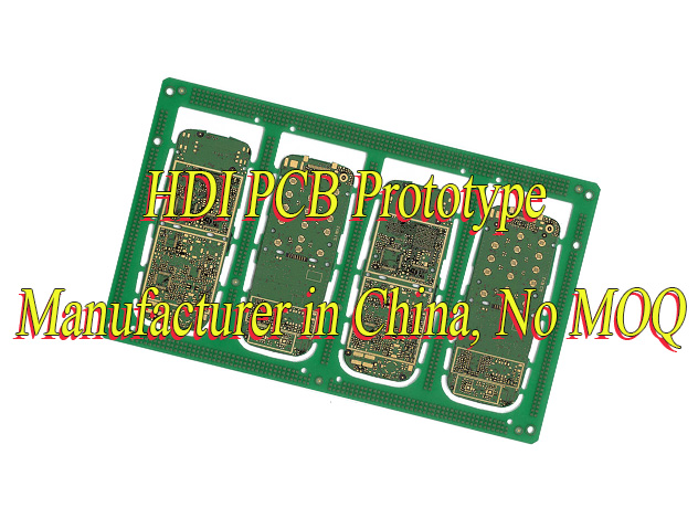
Why do HDI PCB prototype? Let’s discover definition, benefits, design technical parameter, manufacturing processes, cost and lead time for HDI PCB prototypes.
Are you troubled with these problems?
- Are you struggling with yield fluctuations and soaring costs due to line width/spacing breaking the 30μm limit in HDI PCB production?
- Have you encountered interlayer alignment deviations in multi-layer HDI PCBs, causing signal loss and unstable performance?
- Are repeated product testing failures and extended time-to-market caused by high-frequency signal attenuation and crosstalk issues?
As a HDI PCB prototype manufacturer, EBest Circuit (Best Technology) can provide you service and solutions:
- Line Width/Spacing Precision Control – Utilizing imported laser drilling equipment to achieve ±2μm line width/spacing accuracy, maintaining over 98% yield stability and optimizing costs by 15%. Extreme design no longer means cost nightmares.
- Intelligent Interlayer Alignment Optimization – Leveraging AI-assisted design software for ±10μm interlayer alignment precision, reducing signal loss by 20% and improving performance stability by 30%. Multi-layer HDI alignment becomes precision-engineered.
- Full-Chain Signal Integrity Simulation – Providing end-to-end signal integrity simulation from design to testing, proactively identifying risks of high-frequency attenuation and crosstalk. This accelerates time-to-market by 30%, making ‘first-time success’ the industry standard.
Welcome to contact us if you have any inquiry for HDI PCB design, prototyping, mass production, assembly: sales@bestpcbs.com.
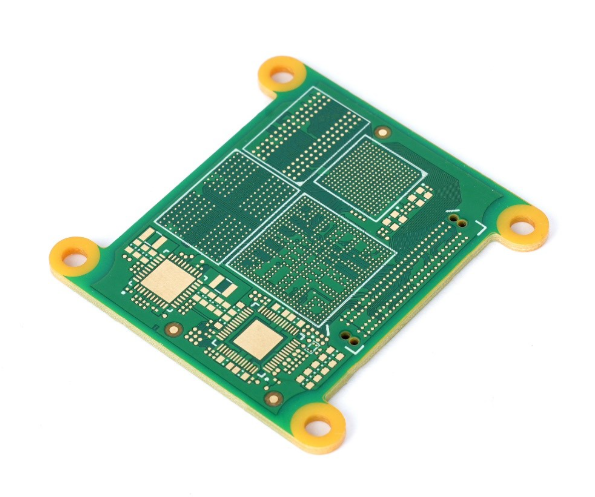
What Is HDI PCB Prototype?
HDI PCB Prototypes are small-batch functional samples produced before mass production to verify the feasibility of high-density interconnect technologies (such as microvias, buried and blind vias, fine line width/spacing, high connection density, and multilayer processes) in specific circuit designs. Their core purpose is to evaluate electrical performance, signal integrity, manufacturing process compatibility, and product reliability through practical testing, promptly identify design flaws, optimize solutions, and ultimately reduce mass production risks. This stage is a crucial step in achieving rapid iteration and risk control in the development of miniaturized, high-performance electronic devices such as smartphones, wearable devices, and high-end servers.
Why Do HDI PCB Prototypes?
Benefits of HDI PCB Prototype:
- Smaller and Lighter: Utilizing microvia technology enables high-density layout, directly helping end products reduce size and weight, improving portability and aesthetics.
- Superior and More Stable Performance: Shorter signal transmission paths and better impedance control significantly improve signal integrity and operational stability in high-speed products.
- More Flexible Design: Provides engineers with greater freedom to place complex chips (such as multi-pin BGAs) within limited space, optimizing overall structural design.
- More Powerful and Richer Functionality: More functional components can be integrated on the same or even smaller board area, enhancing the product’s market competitiveness.
- More Robust and Reliable Connections: Advanced blind and buried via and via-filling processes enhance the board’s mechanical and thermal reliability, making it suitable for demanding application environments.
- Better Overall Cost: While the cost per board may be slightly higher, cost optimization throughout the project lifecycle is achieved through size reduction, improved yield, and accelerated time-to-market.
HDI PCB Prototype Design Technical Parameter
| Parameter Name | Technical Specification/Range |
| Max Layer Count | 4 – 40 layers |
| HDI Stack-up Types | 1+N+1, 2+N+2, 3+N+3, Any-layer |
| Finished Board Thickness | 0.25mm – 3.2mm |
| Min Line Width/Spacing (Inner/Outer) | 2/2 mil (50/50 μm) |
| HDI Substrate Line Width/Spacing | 1.5/1.5 mil (38/38 μm) |
| Min Mechanical Drill Hole Size | 0.15mm |
| Min Laser Drill Hole Size | 0.05mm – 0.1mm |
| Max Aspect Ratio (Through-hole) | 16:1 |
| Dielectric Materials | FR-4, High-Tg, Halogen-free, Polyimide, Rogers, Megtron 6 |
| Min Core Thickness | 2 mil (50μm) |
| Min PP Thickness | 25μm (1017PP) |
| Surface Finishes | OSP, ENIG, ENEPIG, Immersion Tin, Immersion Silver, Electrogold, Gold Finger |
| Special Processes | Resin Plugging, Electroplating Filling, Controlled Depth Drilling, Via-in-Pad (VIPPO) |
| Layer-to-Layer Alignment | ±0.05mm |
| Pad Annular Ring Width | Min 3mil (Through-hole), Min 5mil (Component Hole) |
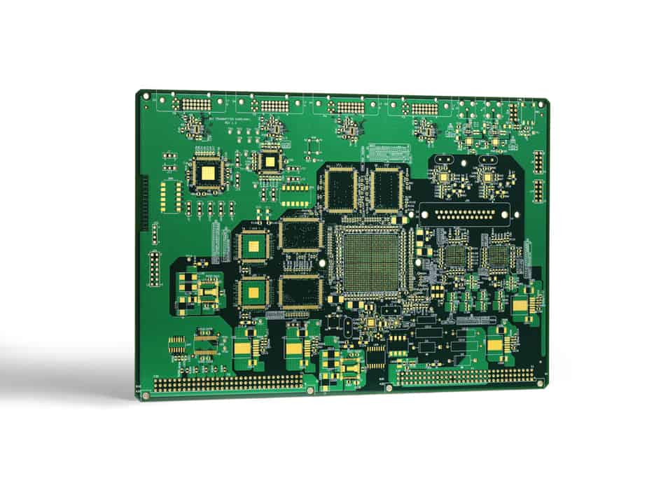
HDI PCB Prototype Manufacturing Processes
1. Design Optimization and Layout Planning
- Use EDA software (such as Altium, Cadence) for circuit design, focusing on optimizing high-density routing. Verify signal integrity through 3D modeling to ensure line width/spacing is controlled within 3-4mil, hole diameter 3-5mil, and meet impedance matching requirements.
- Adopt blind/buried via design to replace traditional through-holes, reducing interlayer signal paths and enhancing space utilization.
2. Material Selection and Pretreatment
- Select low dielectric constant (Dk) and high-frequency performance materials (such as LCP liquid crystal polymer) to reduce signal loss. The substrate uses thin copper foil (typically 0.5-2oz) combined with prepreg for interlayer bonding.
- The pretreatment stage requires chemical copper deposition to ensure uniform copper layer adhesion and enhance conductivity.
3. Inner Core Board Fabrication
- The inner core board forms circuit patterns through photolithography-etching processes. Steps include: cleaning the copper-clad laminate → coating photosensitive dry film → UV exposure to transfer design patterns → developing to remove uncured dry film → alkaline etching to remove exposed copper → stripping and cleaning.
- Use AOI (Automated Optical Inspection) to verify inner layer circuit accuracy, ensuring no short/open circuit defects.
4. Microvia Drilling and Plating
- Employ laser drilling technology (CO₂ laser/UV laser) to fabricate micro blind/buried vias with hole diameters controlled within 50-150μm. Optimize laser parameters to minimize the heat-affected zone (HAZ) and avoid carbonization.
- After drilling, perform plasma cleaning to remove residues, followed by chemical copper deposition + electroplating to form a 25μm thick copper layer, ensuring uniform via wall conductivity.
5. Lamination and Stack-up Structure Construction
- Achieve multi-layer structures through sequential lamination processes. Steps include: core board positioning → stacking (core + prepreg + copper foil) → vacuum hot press curing under high temperature and pressure. Control lamination temperature (170-200°C) and pressure (300-500psi) to ensure no interlayer bubbles/cracks.
- Adopt symmetric stack-up design to reduce board warpage and improve mechanical stability.
6. Outer Layer Circuit Formation
- The outer copper foil forms circuit patterns through photolithography-etching processes, similar to inner layers but using positive film processes.
- Steps include: coating photosensitive film → exposure and development → electroplating to thicken copper layer (to 25μm) → etching to remove excess copper → stripping tin to protect circuits. Use flying probe testing to verify outer layer electrical connections, ensuring no open/short circuits.
7. Surface Treatment and Impedance Control
- Select surface treatment processes (such as ENIG, OSP, gold plating) based on application requirements to enhance soldering reliability. Perform impedance testing in critical areas to ensure signal integrity.
- Adopt differential pair routing + ground plane optimization to control crosstalk and electromagnetic interference (EMI).
8. Reliability Testing and Quality Verification
- Conduct thermal cycling tests (-55°C to 150°C), vibration tests, and X-ray inspections to verify microvia integrity. Analyze via wall filling quality through metallographic sectioning to avoid voids/delamination defects.
- Perform electrical performance tests (such as flying probe testing) to ensure products meet design specifications.
9. Prototype Cutting and Packaging
- Use CNC or laser cutting to segment large panels into individual PCB prototypes, with edge chamfering to prevent damage.
- Clean to remove residual chemicals, and vacuum package to prevent moisture/dust. Attach quality inspection reports containing test data and process parameters for customer verification.
How Much Does HDI PCB Prototyping Cost?
The prototyping cost for HDI (High-Density Interconnect) PCBs typically spans $200 to $2,500+, contingent on complexity and specifications. For basic HDI (4–6 layers, standard FR4), 4-layer HDI PCB cost $200–$600 per panel, while 6-layer options range from $400–$900. Advanced HDI (8+ layers with microvias or high-frequency materials) starts at $800–$2,500+ per panel, with blind/buried vias adding $100–$300 and expedited turnaround (3–5 days) incurring a 30–50% premium.
How Long Does HDI PCB Prototyping Take?
The prototyping lead time for HDI PCBs (High Density Interconnect Printed Circuit Boards) is significantly influenced by factors such as complexity, layer count, via stages, manufacturer capacity, and current order backlog, typically ranging from 3 to 7 working days. For simple HDI designs (1-stage, 6-8 layers), mainstream fast-turn manufacturers can usually complete prototypes within 3-5 working days. Medium-complexity HDI (2-stage, 8-12 layers) extends this to approximately 5-7 working days. High-complexity HDI (3-stage or above, 12+ layers with microvias/fine lines) involves multiple process steps including sequential lamination, laser drilling, via filling/plating, and engineering preparation, requiring 7-15 working days or longer depending on specific technical requirements and factory scheduling. Pricing varies based on design specifications, material costs, and production volume.
Why Choose EBest Circuit (Best Technology) as HDI PCB Prototype Manufacturer?
Reasons why choose us as HDI PCB prototype manufacturer:
- 19 Years of HDI Expertise: Proven track record with 20,000+ complex projects, including 3-stage HDI, 0.1mm microvias, and high-speed materials, achieving 98% first-pass success for intricate designs.
- Zero-Risk Design Assurance: Complimentary DFM analysis intercepts 90% of design flaws upfront, slashing 3-5 design iterations and saving 2-4 weeks of development time, turning R&D budgets into tangible progress.
- Global Compliance & Sustainability: RoHS/REACH-compliant manufacturing, UL certification, and ISO 14001 environmental management, ensuring seamless market access from EU to North America.
- 48-Hours Rapid Prototyping: Standard HDI prototypes shipped within 48 hours—50% faster than industry averages to accelerate your product launch and seize market opportunities.
- Cost Optimization Mastery: Process innovation and vertical supply chain integration cut costs by 15-30% vs. market rates, saving clients up to $5,000+ per project on equivalent specifications.
- Ultra-Reliable Quality Control: Triple-layer inspection (in-line AOI + offline X-ray + first-article validation) achieves ≥99.2% yield rates, exceeding IPC Class 2 standards and minimizing field failure risks.
- Full-Spectrum HDI Capability: From 1-stage to 5-stage HDI processes, supporting 2-32 layer stacks and specialized applications (medical/aerospace/5G) for perfect design-to-production alignment.
- Material Versatility: 20+ material options from standard FR4 to high-speed substrates (e.g., Rogers 4350B) and high-Tg laminates, optimized for performance-cost balance.
- 24/7 Dedicated Engineering Support: 1:1 expert guidance from design consultation to mass production tracking, with 2-hour response, 4-hour solution delivery, and 24-hour issue resolution.
Our HDI Printed Circuit Board Capabilities
| Item | Capabilities |
| Layer Count | 1 – 32 Layers |
| Max Board Dimension | 2424″ (610610mm) |
| Min Board Thickness | 0.15mm |
| Max Board Thickness | 6.0mm – 8.0mm |
| Copper Thickness | Outer Layer: 1oz~30oz, Inner Layer: 0.5oz~30oz |
| Min Line Width/Line Space | Normal: 4/4mil (0.10mm); HDI: 3/3mil (0.076mm) |
| Min Hole Diameter | Normal: 8mil (0.20mm); HDI: 4mil (0.10mm) |
| Min Punch Hole Dia | 0.1″ (2.5mm) |
| Min Hole Spacing | 12mil (0.3mm) |
| Min PAD Ring(Single) | 3mil (0.075mm) |
| PTH Wall Thickness | Normal: 0.59mil (15um); HDI: 0.48mil (12um) |
| Min Solder PAD Dia | Normal: 14mil (0.35mm); HDI: 10mil (0.25mm) |
| Min Soldermask Bridge | Normal: 8mil (0.2mm); HDI: 6mil (0.15mm) |
| Min BAG PAD Margin | 5mil (0.125mm) |
| PTH/NPTH Dia Tolerance | PTH: ±3mil (0.075mm); NPTH: ±2mil (0.05mm) |
| Hole Position Deviation | ±2mil (0.05mm) |
| Outline Tolerance | CNC: ±6mil (0.15mm); Die Punch: ±4mil (0.1mm); Precision Die: ±2mil (0.05mm) |
| Impedance Controlled | Value>50ohm: ±10%; Value≤50ohm: ±5ohm |
| Max Aspect Ratio | 0.334027778 |
| Surface Treatment | ENIG, Flash Gold, Hard Gold Finger, Gold Plating(50mil), Gold finger, Selected Gold plating, ENEPIG, ENIPIG; HAL, HASL(LF), OSP, Silver Immersion, Tin Immersion |
| Soldermask Color | Green/White/Black/Yellow/Blue/Red |
Our Lead Time for HDI PCB Prototype
| Layers | Normal Service | Fastest Service |
| 1 | 7 Days | 24 H |
| 2 | 8 Days | 24 H |
| 4 | 10 Days | 48 H |
| 6 | 10 Days | 72 H |
| 8 | 12 Days | 72 H |
| ≥10 | TBD | TBD |
How to Get a Quote for HDI PCB Prototype?
List of Required Documents for HDI PCB Prototype Quotation
- Gerber Files: Include layer-wise graphics (top/bottom copper layers, solder mask, silkscreen, etc.) in RS-274X format. Must contain individual layer files (e.g., .GTL, .GBL) and drilling layer.
- Drilling Files: Excellon format (.DRL), specifying hole coordinates, sizes, types (through-hole/blind/buried), and slot information.
- Bill of Materials (BOM): List component models, specifications, quantities, and suppliers in formats like .xls/.csv for procurement and assembly.
- PCB Design Source Files: Original design files (e.g., Altium Designer .brd, KiCad .kicad_pcb) as supplementary references to Gerber files.
- Assembly Coordinate Files: Component position coordinates (X, Y) and orientation for SMT placement accuracy.
- Process Specification Document: Details on substrate material (FR4/high-frequency/aluminum), board thickness, copper thickness, surface finish (OSP/HASL/ENIG), solder mask/silkscreen colors, minimum trace/space, impedance control requirements, etc.
- Quantity & Lead Time: Clear production volume and delivery date, influencing quotation and scheduling.
- Testing Requirements: Such as flying probe testing, fixture testing, impedance test reports, etc., to ensure product quality compliance.
- Special Requirements: RoHS compliance, lead-free process, appearance standards, packaging methods, panelization design (e.g., V-cut/stamp holes), etc.
Welcome to contact us if you have any request for HDI PCB Prototype: sales@bestpcbs.com.
Tags: HDI PCB, HDI PCB Prototype, HDI PCB Prototype Manufacturer