

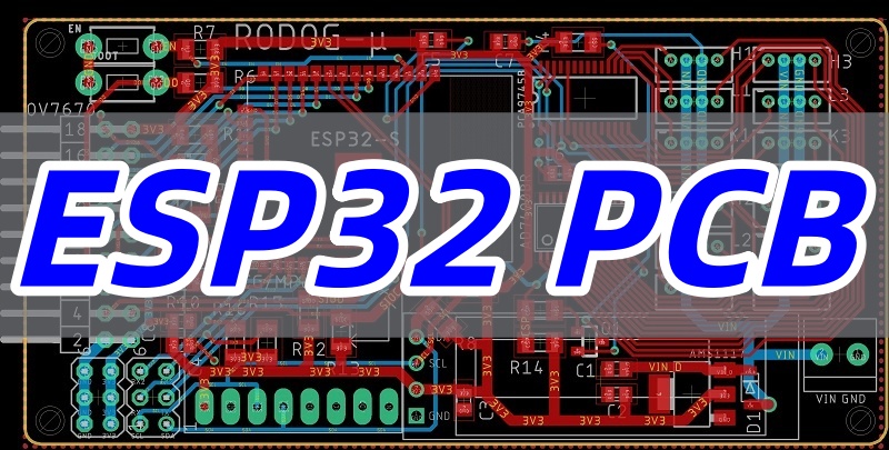
ESP32 PCB is the foundation of countless smart devices. This guide explores its design, features, and how a custom board can power your next IoT project.
Do you ever feel stalled bringing your brilliant IoT idea to life?
- Complex Design Rules: The high-speed and wireless nature of the ESP32 makes circuit board layout tricky. A small error can ruin Wi-Fi or Bluetooth performance.
- Component Sourcing Headaches: Finding genuine, high-quality components for your PCB can be difficult and time-consuming.
- Signal Integrity Issues: Without careful planning, noise can disrupt the ESP32’s sensitive analog and radio functions.
- Manufacturing Misunderstandings: Not knowing a manufacturer’s capabilities can lead to designs that are expensive or impossible to build.
- Thermal Management Problems: Overheating can cause your device to crash or fail prematurely, especially in compact designs.
Fortunately, these challenges have complete solutions. Partnering with an experienced PCB manufacturer transforms these obstacles into a smooth path to a finished product.
- Expert Layout Guidance: We assign engineers who understand RF (Radio Frequency) principles. They ensure your ESP32 PCB layout meets all critical design rules for optimal performance.
- Reliable Supply Chain: We have established relationships with component suppliers. This guarantees we source authentic parts for your custom ESP32 PCB.
- Advanced Design Analysis: Our team uses sophisticated tools to check for signal integrity problems before production. This proactive approach saves time and cost.
- Design for Manufacturing (DFM) Check: We provide a free DFM review. We ensure your ESP32 PCB design is optimized for a smooth and cost-effective manufacturing process.
- Thermal Solution Integration: We help design the board stack-up and copper layers to effectively dissipate heat, ensuring long-term reliability.
EBest Circuit (Best Technology) is a professional PCB manufacturer with deep expertise in IoT projects. Our team provides end-to-end support, from reviewing your ESP32 PCB schematic to delivering high-quality boards. Pls feel free to contact us at sales@bestpcbs.com to discuss your project.
What is ESP32 PCB?
If you’re moving beyond the prototyping stage, you need to understand what an ESP32 PCB truly is. It’s the critical transition from a generic development board to a specialized, functional product.
An ESP32 PCB is a custom-designed printed circuit board that transforms the raw ESP32 chip from a component into a complete, embedded system. Think of it this way:
- The ESP32 Chip is the Brain. It’s a powerful microprocessor with Wi-Fi/Bluetooth.
- The Custom PCB is the Body. It provides the skeleton, nervous system, and interfaces this brain needs to function in the real world.
While a dev board like the ESP32-DevKitC is a fantastic all-in-one toolbox for testing and learning, a custom PCB is a precision-engineered instrument designed for one specific task.
The Key Difference: Dev Board vs. Custom ESP32 PCB
| Feature | Development Board (e.g., ESP32-DevKitC) | Custom ESP32 PCB |
|---|---|---|
| Purpose | Learning, Prototyping, General Use | Final Product, Mass Production |
| Size & Form | Large, fixed size with unused features | Compact, minimal, shaped for your product’s enclosure |
| Cost (at volume) | High per unit | Drastically lower per unit |
| Components | Includes everything, even what you don’t need | Only the essentials for your application |
| Optimization | Generic performance | Highly optimized for power, signal integrity, and thermal management |
When we design a custom board, we’re building a complete ecosystem around the ESP32. Here’s what that actually includes:
- Power Management Circuitry: This is not just a simple USB port. We design robust power regulation (like LDOs or DC-DC converters) to provide clean, stable voltage to the ESP32 and all peripherals, even from a noisy battery source.
- Memory & Storage: We add the necessary Flash memory and PSRAM based on your firmware’s requirements, ensuring reliable operation without bloat.
- The Antenna Ecosystem: This is a major differentiator. We integrate the antenna—either a PCB trace antenna, a ceramic chip antenna, or an u.FL connector for an external antenna—and design the matching network for optimal Wi-Fi/BT range.
- Peripheral Interfaces: We break out the necessary GPIOs to dedicated headers or connectors for your specific sensors (I2C, SPI, ADC), actuators, displays, and other components.
- Programming & Debugging: We include a compact, cost-effective programming interface (like a simple serial header) for factory flashing and future updates, unlike the bulky USB-to-Serial chip on dev boards.
In essence, a custom ESP32 PCB is the process of distilling a general-purpose prototype into a sleek, reliable, and cost-effective final product. It’s what allows your smart device to be manufactured efficiently and perform reliably in the field.
For a client, the decision to create a custom ESP32 PCB is the decision to professionalize your invention. It’s the key to reducing size, slashing costs, and ensuring the robust performance that customers expect. At EBest Circuit (Best Technology), we specialize in guiding you through this exact process, turning your proven concept into a manufacturable reality.
What are the Features of PCB ESP32?
The features of a PCB built for the ESP32 are what make it so powerful for IoT. They go far beyond just holding the chip.
- Robust Power Design: A good board includes a stable voltage regulator. It ensures the ESP32 gets clean power even when the battery is low or input voltage fluctuates.
- Optimized RF Layout: This is perhaps the most critical feature. The ESP32 PCB antenna design is carefully planned. Proper grounding and trace routing prevent interference. This gives you the best possible Wi-Fi and Bluetooth range.
- Rich Connectivity Options: The PCB breaks out the ESP32’s many pins. This allows for easy connection to sensors, displays, and motors. You can find headers for I2C, SPI, UART, and GPIOs.
- Efficient Thermal Management: The board itself helps cool the chip. Thermal vias and large copper pours pull heat away from the ESP32. This prevents overheating during intense tasks.
- Compact Form Factor: A custom ESP32 PCB can be made very small. This is perfect for fitting into wearable devices or other space-constrained applications.
These features work together to create a reliable foundation for any connected device.
What’s Function of ESP32 on PCB?
The ESP32 chip on the PCB is the command center. Its job is to process information and make decisions.
- First, it connects to the internet or other devices via its built-in Wi-Fi and Bluetooth.
- Then, it reads data from sensors connected to the PCB, like a temperature sensor. After that, it processes this data.
- Finally, it acts on it—for example, by sending a command to an actuator or transmitting the data to the cloud.
The ESP32 on PCB orchestrates all the electronic components around it. It turns a simple board into a smart, connected device.
What is an ESP32 Board Used for?
Understanding the applications of the ESP32 is the first step. The core strength of the ESP32—its low cost and wireless connectivity—is fully unlocked only when it’s packaged efficiently for its specific task. Let’s explore the common use cases, with a focus on what moving to a custom PCB makes possible.
1. Smart Home & Building Automation
- Example Devices: Smart light switches, thermostats, leak sensors, and smart plugs.
- The Dev Board Limitation: A generic dev board is too large and expensive to fit inside a standard light switch wall plate. It also includes unnecessary components, wasting space and money.
- The Custom PCB Advantage: We design a compact, shape-optimized board that fits perfectly into the product’s enclosure. The design is optimized for low power consumption, allowing battery-powered sensors to last for years. This is where a robust ESP32 PCB layout for power efficiency is critical.
2. Industrial Monitoring & Control
- Example Devices: Machine health monitors, environmental sensors (temperature, humidity, VOC), and asset trackers.
- The Dev Board Limitation: Dev boards are not designed for harsh industrial environments. They are vulnerable to electrical noise, vibration, and temperature fluctuations, leading to crashes and data loss.
- The Custom PCB Advantage: We can build ruggedized boards with conformal coating, robust power conditioning to handle noise, and secure mounting points. For an ESP32 drone PCB used in agricultural surveying, the board must be lightweight yet resilient to vibration. This level of reliability is impossible with a standard dev board.
3. Consumer Gadgets and Wearables
- Example Devices: Fitness trackers, smart watches, and connected toys.
- The Dev Board Limitation: A dev board is bulky, power-hungry, and aesthetically unworkable for a wearable device.
- The Custom PCB Advantage: We can create tiny, flexible, or rigid-flex boards that contour to the wearable’s form factor. Power management is meticulously designed for maximum battery life. The ESP32 PCB antenna design is optimized to perform well even when close to the human body. This is a hallmark of professional ESP32 custom PCB design.
4. Agriculture and Environmental Sensing
- Example Devices: Soil moisture networks, weather stations, and automated irrigation controllers.
- The Dev Board Limitation: These devices are often deployed in remote, outdoor locations. Dev boards lack the necessary weatherproofing and long-range connectivity options.
- The Custom PCB Advantage: We can design boards with enclosures that are sealed against moisture and dust. The RF layout can be optimized for a specific antenna (e.g., a high-gain external antenna) to maximize the wireless range in open fields, a key consideration in any ESP32 PCB design guide.
5. High-Performance Hobbyist Projects
- Example Devices: The WLED ESP32 PCB for complex LED arrays, the ESP32 marauder PCB for wireless security testing, or the ESP32 cam PCB for high-quality video streaming.
- The Dev Board Limitation: While hobbyists start with dev boards, advanced projects demand custom PCBs to integrate specialized components, improve signal integrity for video streams, or create a professional-looking final product.
- The Custom PCB Advantage: We help hobbyists and prosumers bridge the gap to a polished product. A custom PCB with ESP32 allows for the perfect integration of all components, resulting in better performance and a more marketable end-unit.
The shift from a standard ESP32 board to a custom ESP32 PCB is the shift from “it works” to “it works perfectly in its intended environment.” It’s about optimizing for:
- Cost at volume
- Size and Form Factor
- Power Consumption
- Reliability and Ruggedness
- Performance (RF range, signal integrity)
At EBest Circuit (Best Technology), we don’t just manufacture your PCB; we help you identify these optimization points. We use our expertise to ensure your ESP32 PCB schematic and layout are tailored for your application’s unique challenges, turning a great idea into a viable, manufacturable product.
ESP32 PCB Footprint Best Practices
The footprint is the pattern of copper pads on the PCB where the ESP32 chip is soldered. Getting this right is non-negotiable. A bad footprint can lead to poor soldering and device failure.
- Follow the Datasheet: Always use the official ESP32 PCB footprint from Espressif’s datasheet. Do not try to create it from scratch. This ensures the pad sizes and spacing are perfect.
- Use Correct Solder Mask: The solder mask should have a tight opening around the pads. This prevents solder from bleeding and creating short circuits during assembly.
- Include a Courtyard: Add a keep-out area around the footprint. This ensures no other components are placed too close, which helps with soldering and inspection.
- Thermal Pad Design: Many ESP32 modules have a large thermal pad underneath. The footprint must have a corresponding pad with multiple vias. This helps transfer heat into the ground plane of the PCB.
- Reference Designator: Clearly label the footprint on the silkscreen. This helps during assembly and any future debugging.
Using a library like ESP32 PCB KiCad or ESP32 PCB design EasyEDA can help. These often include pre-verified footprints. This saves time and prevents errors.
Where to Get PCB for ESP32?
Navigating the path from an ESP32-based idea to a functional printed circuit board (PCB) can be complex. The right sourcing strategy depends heavily on your project’s stage, volume, and performance requirements. This guide breaks down the options, highlighting why a partnership with a specialist manufacturer like EBest Circuit (Best Technology) is crucial for moving beyond the prototyping phase into successful mass production.
1. For Prototyping: Pre-made Development Boards
The fastest way to start developing with the ESP32 is to use a pre-assembled development board (e.g., from SparkFun or Adafruit). These are excellent for software development, proof-of-concept testing, and small-scale projects. However, they are often larger, more expensive per unit, and may include features unnecessary for your final product, making them unsuitable for commercial volume production.
2. For Custom Products & Commercialization: Custom PCB Manufacturing with EBest Circuit (Best Technology)
When you’re ready to productize your design, you need a custom PCB. This involves two critical steps:
- Design: You create the schematic and layout using ECAD software. Open-source platforms like ESP32 PCB GitHub repositories can offer valuable reference designs.
- Fabrication: You send your design files (Gerbers) to a PCB manufacturer. This is where the choice of partner becomes paramount.
While online “board houses” offer low-cost prototyping, they often lack the specialized expertise for a successful, high-performance ESP32 product. For a reliable, wireless-enabled device, you need a manufacturer with specific capabilities in impedance control, RF layout, and signal integrity—this is where EBest Circuit (Best Technology) excels.
EBest Circuit (Best Technology) bridges the gap between a basic design and a high-performance product. We don’t just manufacture your board; we provide expert Design for Manufacturability (DFM) analysis, ensuring your ESP32 PCB schematic and layout are optimized for reliability and performance from the start. Our support throughout the process de-risks your journey from concept to a finished, market-ready ESP32 PCB board.
Our specific capabilities for ESP32 PCBs include:
- Advanced RF and Manufacturing Expertise: ESP32 designs demand precise control over impedance and RF characteristics. Our manufacturing processes are equipped to handle these requirements, ensuring stable wireless performance. We support complex multi-layer boards (up to 32 layers) which are often necessary for sophisticated ESP32-based products that integrate numerous functionalities.
- Precision Engineering for High Density: We achieve fine line widths and spacing, with capabilities for outer layer lines down to 3.5/4 mil and inner layers down to 3/3 mil. This precision is essential for routing the dense BGA packages of modern ESP32 modules and maintaining signal integrity for high-speed interfaces like USB OTG on the ESP32-S3.
- Comprehensive Surface Treatment Options: To ensure the best solderability and long-term reliability for your ESP32 board, we offer a variety of surface finishes suitable for RF applications, including ENIG (Immersion Gold), OSP, and Immersion Silver. We advise against HASL (Hot Air Solder Leveling) for fine-pitch ESP32 designs due to potential flatness issues.
- Rigorous Quality Control: We adhere to strict quality standards, performing electrical testing to verify 100% connectivity (using either flying probe for prototypes or test fixtures for mass production) and inspecting against IPC-A-600 class 2/3 acceptance criteria to guarantee a reliable final product.
By leveraging our extensive manufacturing experience and technical capabilities, EBest Circuit (Best Technology) is the ideal partner to transform your ESP32 design into a robust, high-performance reality.
Technical Capability of Custom ESP32 PCB – EBest Circuit (Best Technology)
Designing a PCB for a high-speed, wireless module like the ESP32 demands precision engineering. EBest Circuit (Best Technology) possesses the advanced technical infrastructure and expertise to meet these stringent requirements.
1. Support for Complex Designs and Tools:
We are agnostic to your design environment, seamlessly handling files from all major ECAD software, including designs made with ESP32 PCB layout Proteus. Our engineers are adept at working with your design files to ensure a smooth transition to production.
2. Critical High-Frequency and RF Expertise:
The core of a successful ESP32 design lies in its radio frequency (RF) performance. Our capabilities are tailored for this challenge:
- Advanced Layer Counts: We can manufacture boards with up to 12 layers, essential for complex products requiring dense component placement and multiple power domains while maintaining signal integrity.
- Impedance Control: We strictly control impedance for high-speed data lines (like those for ESP32-S3’s USB OTG) to prevent signal reflection and data corruption. Our process controls impedance tolerance within ±10%, which is critical for stability.
- ESP32 PCB Antenna Design: This is a critical differentiator. We expertly manage the antenna layout, ensuring optimal placement away from noise sources and proper grounding to maximize wireless range and connectivity reliability. Our ESP32 PCB design guide incorporates best practices for antenna matching circuits and keep-out areas.
3. Precision Manufacturing and Quality Assurance:
Our manufacturing prowess, as detailed in our capability charts, ensures the highest quality:
- Fine Line Technology: We achieve inner layer line widths/spacing down to 2.5/2.5 mil and outer layer down to 3/3 mil, allowing for dense and efficient layouts.
- Diverse Materials: We work with standard FR-4 as well as high-speed/low-loss materials (e.g., TU-872SLK, IT-968) suitable for demanding RF applications, ensuring minimal signal loss (Df).
- Rigorous Testing: Every board undergoes electrical testing for shorts and opens (E-test). We offer both flying probe for prototypes and test fixture testing for volume production, guaranteeing 100% functionality before shipment.
By leveraging these capabilities, we transform your custom ESP32 PCB design into a robust, high-performance reality, fully compliant with IPC standards.
Case of ESP32 Drone PCB Manufacturing at EBest Circuit (Best Technology)
This project showcases EBest Circuit (Best Technology)’s expertise in manufacturing a high-complexity, 8-layer rigid-flex PCB for a cutting-edge industrial inspection drone.
Application Scenario
The board serves as the core flight controller. Based on the ESP32-S3, it required robust wireless communication for real-time telemetry and HD video transmission. The rigid-flex design was critical: the rigid sections house the main processor and sensitive sensors, while the flexible portions allow the board to conform to the drone’s compact, irregular airframe, ensuring reliability under extreme vibration and EMI conditions.
PCB Specifications & Key Parameters
The board was built to the following precise specifications, demonstrating our manufacturing capabilities:
- Board Type: 8-Layer Rigid-Flex PCB
- Base Material: FR-4, High Tg 170
- Board Thickness: Rigid Section: 1.1mm ±0.11mm / Flex Section: 0.22mm ±0.05mm
- Copper Weight: 1 oz (Inner/Outer Layers)
- Plated Through-Hole (PTH) Copper: 25µm ±5µm
- Surface Finish: Flexible Area: 1mil Black Coverlay / Rigid Area: Black Solder Mask, White Silkscreen
- Special Process: Via-in-Pad with Resin Filling
- Impedance Control: Controlled Impedance, ±10% tolerance
- Flex Core: 2mil Adhesiveless PI
This project leveraged several of our advanced technical competencies:
- Rigid-Flex Lamination Expertise: Precise control during the lamination process was essential to bond the rigid and flexible materials seamlessly without delamination.
- Impedance Control & Signal Integrity: Our engineers meticulously controlled the impedance for the high-speed signals from the ESP32-S3, including the Wi-Fi RF lines and USB OTG differential pairs, ensuring stable data transmission.
- Advanced Drilling & Plating: Achieving reliable PTH vias in the rigid-flex interface requires specialized drilling and plating techniques to ensure connectivity and mechanical strength.
- Via-in-Pad and Resin Filling: This process was critical for the fine-pitch BGA components, creating a flat surface for soldering and enhancing reliability.
In conclusion, the ESP32 PCB is the unsung hero of the IoT revolution, providing the solid foundation upon which smart devices are built. This article has explored its design, function, and the immense potential of creating a custom board.
EBest Circuit (Best Technology) has the technical expertise and manufacturing precision to deliver high-quality ESP32 PCBs that perform. We help you navigate the complexities of RF design and thermal management. Pls feel free to send us your design files or questions anytime. Contact our team at sales@bestpcbs.com. We are here to help.
Tags: ESP32 PCB