

Why choose high frequency PCB for RFID readers? Let’s discover its benefits, applications, material selection, design technical parameter, design optimize solutions, recommended PCB manufacturer.
Are you worried about these problems?
- How to select high frequency PCB board materials?
- How to control high frequency PCB board processes?
- How to balance cost vs lead time of high frequency PCB?
As a high frequency PCB manufacturer, EBest Circuit (Best Technology) can provide services and solutions:
- Low-loss Material Supply: Stocked PTFE/Rogers laminates ensure stable dielectric constant (Dk≤3.0), reducing signal loss by 40%+.
- Precision Impedance Control:±0.02mm trace width tolerance maintains ≤5% impedance variation for flawless signal transmission.
- Rapid-response Flexible Production: Prototypes in 5-7 days, bulk order lead time shortened by 30% with 15%+ cost optimization.
Welcome to contact us if you have any inquiry for high-frequency PCB board: sales@bestpcbs.com.
Why Choose High Frequency PCB for RFID Readers?
Reasons why choose high frequency PCB for RFID readers:
- Breakthrough in Reading Distance: Adopting low-loss substrates like Rogers RO4350B reduces signal transmission loss by 40%, enabling UHF-band reading distances exceeding 12 meters, ideal for large-scale logistics and warehouse scanning.
- Enhanced Anti-Interference Capability: Optimized microstrip layout and multi-layer shielding grounding meet ETSI EN 302 208 standards, improving signal stability by 60% in industrial electromagnetic environments.
- High-Speed Signal Integrity: Precise 50Ω impedance matching and decoupling capacitor configurations ensure data transmission rates up to 100Mbps, guaranteeing rapid tag response.
- Precision Manufacturing Process: 0.1mm line/space blind-buried via technology with ±5% copper plating thickness tolerance minimizes signal loss and enhances system reliability.
- TCO Optimization Proven: Case studies like DHL show 35% improvement in asset tracking efficiency, 99.2% inventory accuracy, 28% reduction in 5-year maintenance costs, and an 18-month payback period.
- 5G IoT Compatibility: Supports sub-6GHz bands and millimeter-wave integration, complying with 3GPP Release 17 specifications for future smart logistics and autonomous driving scenarios.
- Global Standard Compliance: Passes GS1 certification, IEEE 802.11 compatibility tests, and RoHS material requirements, ensuring seamless global market access.
- Supplier Evaluation Framework: Structured assessment model covering material certification, process capability, testing validation, and case references, providing quantifiable decision-making tools for commercial conversion.
Applications of High Frequency PCB in RFID Readers
- NFC Payment Terminals
- Smart Access Control Systems
- Industrial Sensor Networks
- Large-scale logistics and warehouse scanning
- Smart retail shelf management
- Real-time medical equipment tracking
- Contactless vehicle passage in transportation
- Industrial automation production line control
- Smart city infrastructure monitoring
- Cold chain logistics temperature tracking
How to Choose High Frequency PCB Material for RFID Readers?
1. Three Key Parameters
- Low Dk (≤3.6, e.g., Rogers RO4350B Dk=3.48) reduces signal delay; PTFE (Dk=2.1) suits UHF/mmWave for faster transmission.
- Low Df (≤0.004, e.g., RO4350B Df=0.0037) minimizes signal loss; PTFE (Df=0.001) ensures 5G/6G signal integrity.
- High Tg (≥150°C, e.g., RO4350B Tg=280°C) resists heat; PTFE handles -260°C~260°C for extreme conditions.
2. Scenario-Specific Matching
- UHF (900MHz) uses RO4000 series (low cost, easy processing); 5G/mmWave (24GHz+) selects PTFE (low loss) or ceramic-filled materials (high stability).
- Humid environments choose PTFE (water absorption ≤0.02%); high-temperature scenarios use PI (Tg≥260°C); anti-metal interference requires multi-layer shielding grounding.
3. Cost-Process Balance
- Mid-frequency (≤10GHz) prefers RO4000 series (40% cheaper than PTFE); high-frequency (≥10GHz) uses PTFE (superior performance but 3-5x costlier).
- RO4000 works with FR4 processes (lower equipment investment); PTFE needs specialized tools for precision needs.
4. EMC Compliance Essentials
- Optimized microstrip lines + multi-layer shielding (meets ETSI EN 302 208) suppress 900MHz interference; decoupling capacitors near chip pins ensure clean power.
- Prioritize GS1/IEEE 802.11/RoHS-certified materials; suppliers must provide impedance matching and signal integrity reports.
5. Validation Loop
- Test read distance/anti-interference in real scenarios such as logistics, medical to verify performance.
- Evaluate suppliers’ material certifications (e.g., Rogers authorization), process capabilities (blind/buried via yield ≥98%), and case references for reliable supply chain.
High Frequency PCB Board Design Technical Parameter
| Parameter Category | Specification |
| Dielectric Constant (Dk) | 2.0-3.6 (PTFE substrate down to 2.0-2.2) |
| Dissipation Factor (Df) | 0.0004-0.004 (PTFE down to 0.0004) |
| Glass Transition Temperature (Tg) | 150°C-280°C (RO4350B up to 280°C) |
| Coefficient of Thermal Expansion (CTE) | Matched with components (avoid thermal stress) |
| Water Absorption | ≤0.02% (PTFE) |
| Impedance Control | 50Ω single-ended / 90-100Ω differential (±3%-±5% tolerance) |
| Trace Width/Spacing | Minimum 4mil/4mil (after etching) |
| Dielectric Thickness | 0.1-0.3mm (microstrip dielectric thickness) |
| Copper Foil Type | Electrolytic Copper (ED)/Rolled Annealed Copper (RA) |
| EMC Design | Shield grounding/stitching vias/differential routing |
How to Design High-Frequency PCBs to Optimize the Reading Distance of RFID Readers?
1. Antenna Size & Polarization Optimization
- Size Scaling: 86×54mm large-size tags achieve 12m read range in industrial scenarios (260% improvement vs 35×35mm tags), suitable for large object identification like warehouse pallets.
- Circular Polarization: Spiral/microstrip patch antennas support random tag orientation, improving detection rate from 75% to 98% in logistics sorting.
- Metal Clearance: Maintain ≥10cm spacing between antenna and metal objects; optimized layout reduces read range attenuation by 40% in metal-adjacent scenarios.
2. Low-Loss Material Selection
- Material Comparison: Rogers RO4350B (Dk=3.48/Df=0.0037) reduces signal attenuation by 40% vs FR4 for UHF; Taconic TLY-5 (Dk=2.2/Df=0.002) excels in millimeter-wave for 5G integration.
- Dielectric Constant Control: Dk deviation ≤±0.05 ensures impedance matching precision, minimizing signal reflection loss.
- Moisture Management: PTFE substrates with ≤0.02% water absorption require waterproof coatings or low-absorption materials in humid environments.
3. Stack-Up & Impedance Control
- 6-Layer Structure: TOP (RF signal)-GND-Inner signal-Power-GND-BOTTOM (mmWave signal) ensures tight coupling between signal layers and ground planes, reducing crosstalk.
- Microstrip Design: 50Ω single-ended line width matches 0.1-0.3mm dielectric thickness; differential impedance targets 90-100Ω.
- Tolerance Control: Single-ended impedance deviation ≤±5%, verified via simulation (e.g., Ansys HFSS) and network analyzer calibration.
4. Ground Plane & Power Integrity
- Continuous Ground: Via fences (spacing ≤0.2λ) suppress EM leakage; avoid ground plane splitting to maintain signal integrity.
- Power Decoupling: Parallel 1nF/100nF capacitors reduce power ripple to <50mV; low-noise LDO modules enhance signal purity.
- Ground Bounce Mitigation: Multi-layer ground planes interconnected via metalized vias create low-impedance return paths, reducing ground noise impact.
5. Impedance Matching & Dynamic Tuning
- Smith Chart Matching: LC/π-networks achieve 50Ω matching, improving sensitivity by 2-3dB and restoring ≥3.2m read range in metal environments.
- Calibration: S-parameter testing ensures tuning accuracy; dynamic tuning algorithms adapt to impedance fluctuations from tag position changes.
- Anti-Metal Solutions: Ceramic substrates or absorptive adhesive tags with FHSS combat EM interference, maintaining 99% recognition rates on metal surfaces.
6. Environmental Robustness Enhancements
- Liquid Compensation: Dielectric constant compensation reduces signal attenuation; phased-array antennas minimize 89% blind spots in liquid container detection.
- Thermal Stability: Materials with Tg≥150℃ (e.g., RO4350B Tg=280℃) operate in -40℃~150℃ environments, preventing layer separation or performance degradation.
- Mechanical Optimization: 2oz copper thickness and thermal vias enhance PCB durability against vibration/impact in logistics.
7. System-Level Dynamic Optimization
- Power Adaptation: 0.5W-2W dynamic regulation increases tag recognition from 200 to 800 per read, optimizing multi-tag concurrency.
- Q-Value Anti-Collision: Machine learning predicts optimal read windows, boosting dynamic scene recognition by 40% and reducing missed tags.
- Thermal Management: High-thermal-conductivity materials (e.g., copper substrates) with thermal vias dissipate heat from high-frequency power loss, ensuring stable operation and extended lifespan.
Why Choose EBest Circuit (Best Technology) as High Frequency PCB Manufacturer?
Reasons why choose us as high frequency PCB manufacturer:
- 19 Years of Expertise: 19-year focus on high-frequency PCBs with 5,000+ validated projects. Unique process knowledge base and failure analysis system reduce defect rates by 60% vs industry average.
- Quality Certification: ISO9001/IATF16949/ISO13485 certified, make sure that every process passed ISO quality inspection system.
- 5-7 Days Rapid Prototyping: 5-7 Days prototype delivery for standard high-frequency PCBs; 3-5 Days turnaround for urgent orders. Supports 180+ global regions with 99.2% on-time delivery for urgent R&D needs.
- Advanced Material: Uses low-loss materials like Rogers RO4350B and Taconic TLY-5 (Dk=2.2-3.48, Df=0.0004-0.0037) with dielectric constant tolerance ≤±0.02, reducing signal loss by 40% vs FR4.
- Precision Process Control: High-precision CNC drilling, laser cutting, and automated lines ensure ±0.01mm line width/spacing and ±5% impedance matching accuracy for 50Ω/75Ω standards.
- Cost Advantage: Eco-friendly high-frequency materials cut costs by 40%. Tiered pricing: double-layer boards as low as ¥0.8/piece; six-layer boards under ¥220/m², 30% cheaper than imports.
- Reliability Testing: Endures -40°C to 125°C thermal cycling, humidity shock, and signal loss optimization. Maintains stability in extreme environments (such as space simulation, industrial radar) with <0.1% error rate.
- Turnkey Solutions: Full-service support from circuit design and BOM sourcing to PCB assembly. Reduces overall cycle time by 50% with rapid customization response.
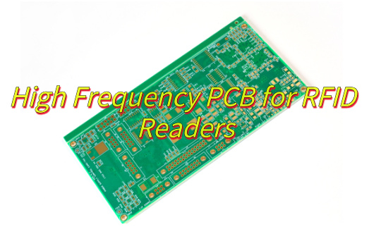
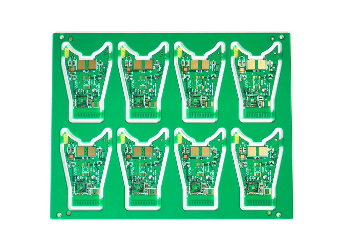
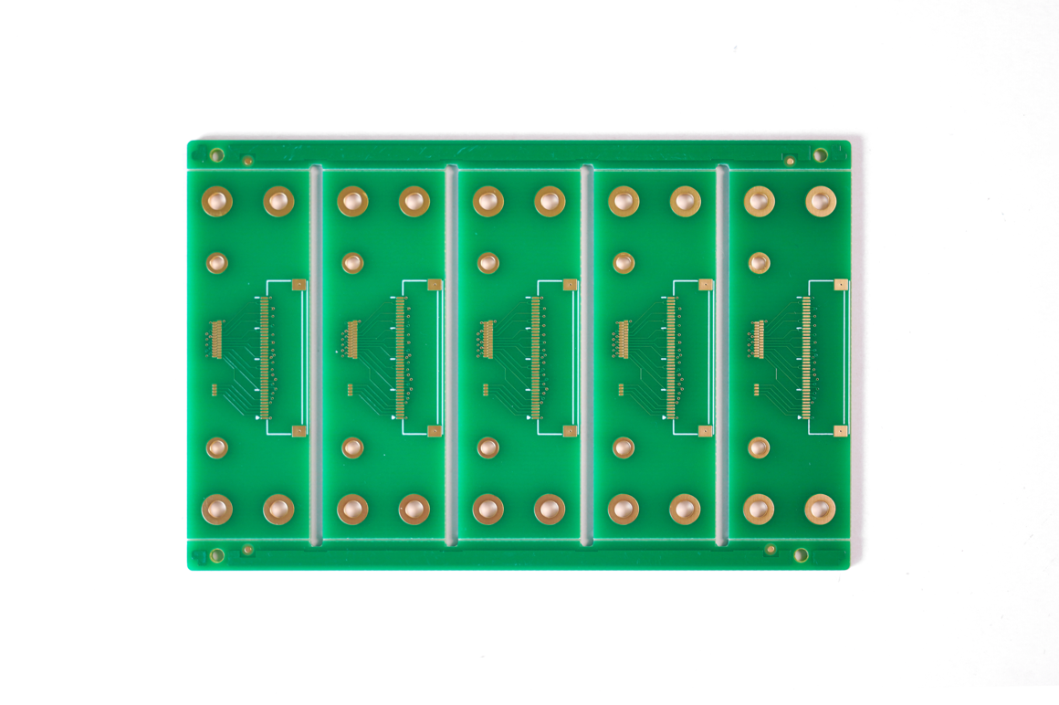
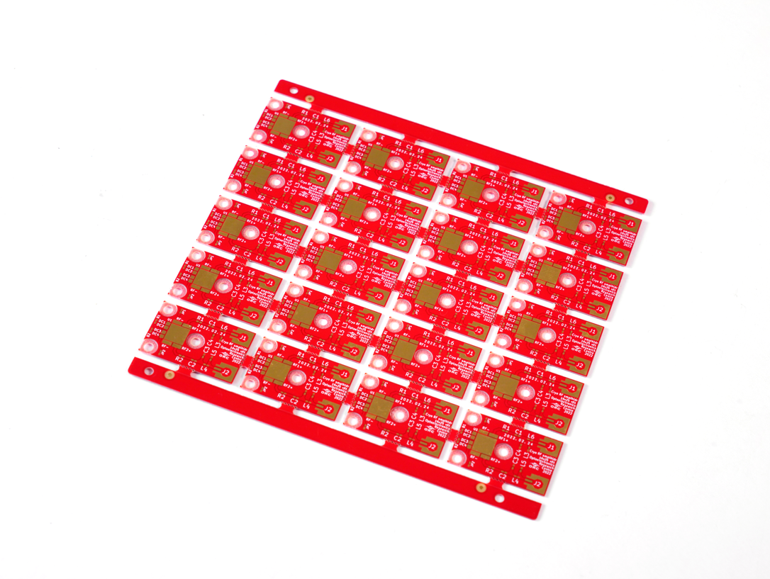
Here is a photo of high frequency PCB we did before:
| Parameter | Specification |
| Substrate Model | Rogers RO4350B (Dk=3.48/Df=0.0037), Taconic TLY-5 (Dk=2.2/Df=0.002) |
| Layer Structure | 4-10 layer multilayer board, supports high-frequency + HDI hybrid process |
| Size Range | 50×50mm to 500×500mm |
| Copper Thickness | 0.5oz-2oz (2oz recommended for high-power areas) |
| Impedance Control | 50Ω±5% (matches RFID antenna standards) |
| Line Width/Spacing | Minimum 75μm/75μm (high-frequency signal transmission precision) |
| Surface Finish | ENIG (Electroless Nickel Immersion Gold), OSP (Organic Solderability Preservative) |
| Special Processes | Blind/buried vias (depth ≤6 layers), backdrilled stub ≤50μm |
| Frequency Range | 13.56MHz / UHF (860-960MHz) |
Our High Frequency PCB Capabilities
| Base material: | Rogers/Telfon |
| Board Thickness: | 0.5mm~3.0mm(0.02″~0.12″) |
| Copper thickness: | 0.5 OZ, 1.0 OZ, 2.0 OZ, 3.0 OZ |
| Outline: | Routing, punching, V-Cut |
| Soldermask: | White/Black/Blue/Green/Red Oil |
| Legend/Silkscreen Color: | Black/White |
| Surface finishing: | Immersion Gold, HASL, OSP |
| Max Panel size: | 600*500mm(23.62″*19.68″) |
| Packing: | Vacuum/Plastic bag |
| Samples L/T: | 7~9 Days |
| MP L/T: | 8~10 Days |
How to Get a Quote for High-Frequency PCB Project?
1. Basic Design Files
- Gerber Files: Include all layers (with drill files), specify version (e.g., RS-274X).
- Stack-up Diagram: Define dielectric thickness, copper thickness, and material type (e.g., Rogers RO4350B, FR4).
- Impedance Control: Mark critical signal impedance values (e.g., 50Ω±10%) and corresponding layers/line widths.
2. Material Specifications
- Substrate Parameters: Dielectric constant (Dk), loss tangent (Df), Tg value (e.g., PTFE substrates).
- Copper Foil Type: Electrolytic/rolled copper, surface roughness requirements (e.g., HVLP copper foil).
- Special Process Needs: Blind/buried vias, laser drilling, high-frequency hybrid stacking.
3. Electrical & EMC Requirements
- Signal Frequency Range: e.g., 2.4GHz/5.8GHz, mark sensitive traces (e.g., RF antenna routing).
- Shielding Design: Metalized via walls or localized shielding cans if required.
- Voltage/Insulation Standards: e.g., IPC-6012 Class 2/3.
4. Surface Finish & Acceptance Criteria
- Surface Treatments: ENIG, Immersion Ag, OSP, etc.
- Acceptance Standards: IPC-A-600 visual grade, impedance test tolerance (e.g., ±5%).
5. Other Key Information
- Lead Time: Sample/mass production timeline requirements.
- Testing Needs: TDR impedance test, RF parameter tests (S-parameters).
- Additional Files: Design notes (special process remarks), BOM (if SMT required).
Welcome to contact us if you have any request for high frequency PCB board: sales@bestpcbs.com.
Tags: high frequency pcb